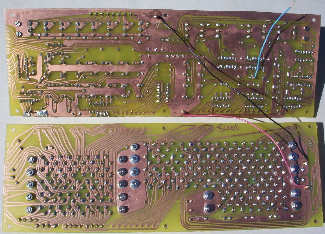
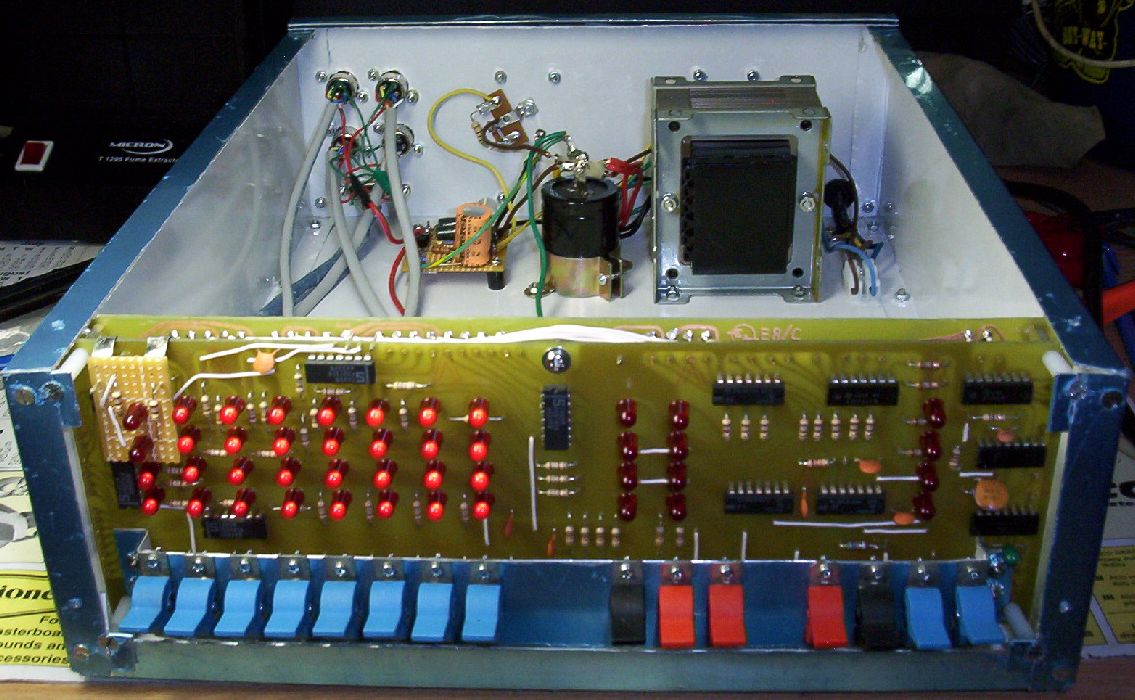
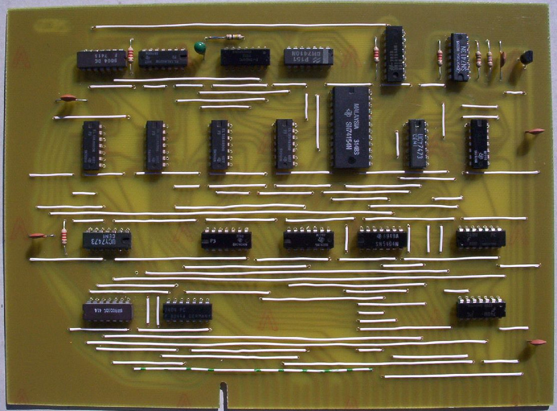
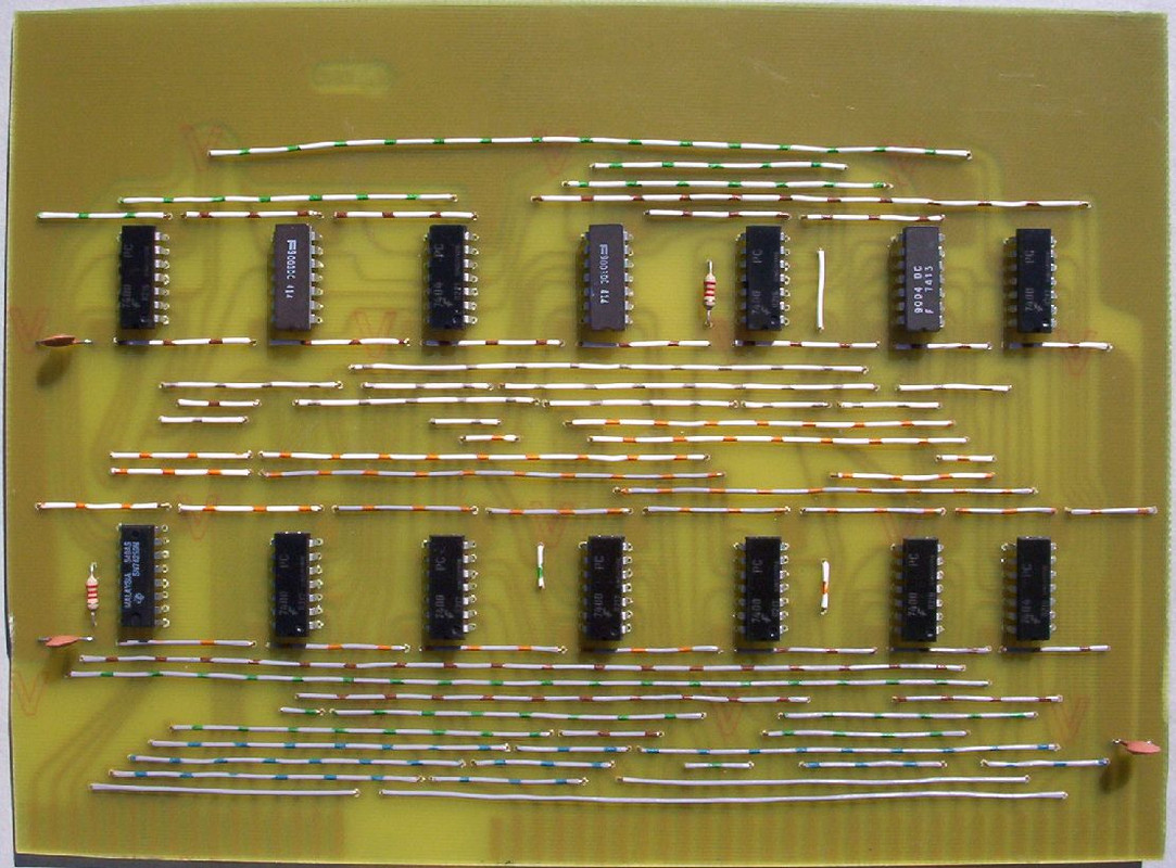
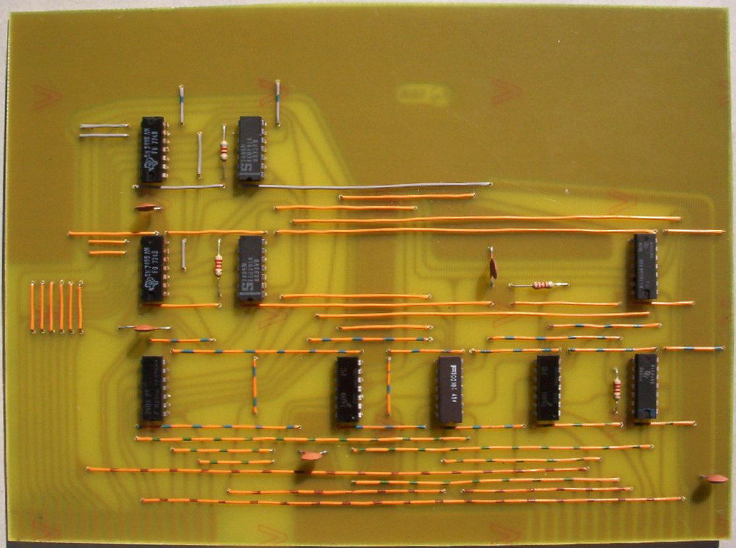
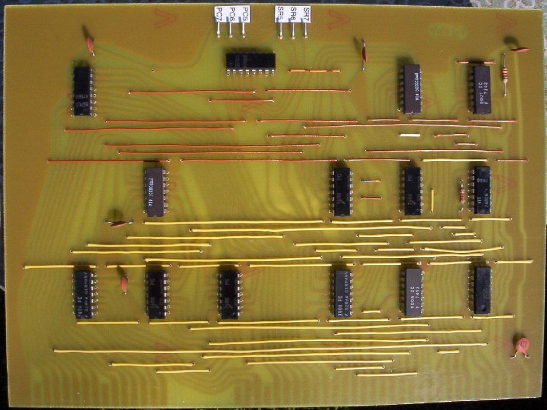
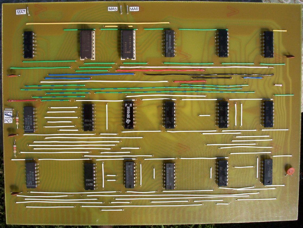
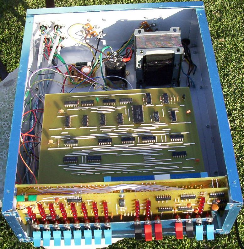
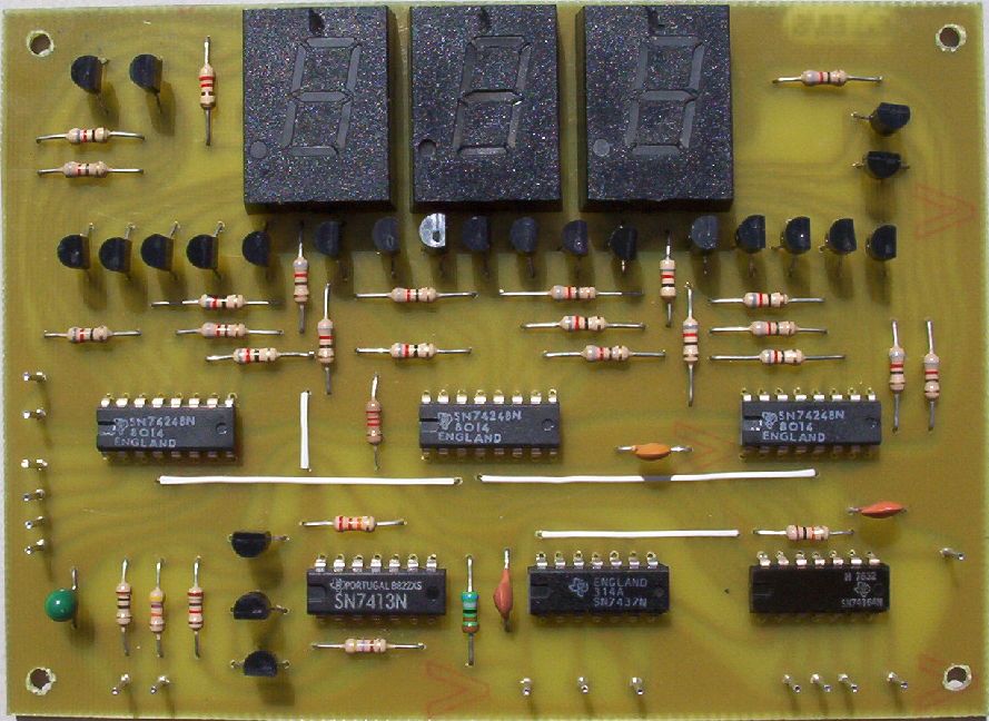
The computer uses a custom power supply, supplying 6A at 5V (30W total) to the computer and peripherals. The computer uses 3A (15W) with the peripherals using up to 3A. The main computer is housed in a 103 x 293 x 357 mm case. There are eight single-sided printed circuit boards consisting of the Front Panel Board, Connector Board, Timing Board, Decoder Board, Accumulator Board, Program Counter and Adder Board, Memory Board, and IOT Interface Board.
In the late 1970's I was in high school and had found the articles in the school library describing how to build the EDUC-8. You could also buy an EDUC-8 as a kit, but is was quite expensive at $300 (about $1200 today). Not having $300, I asked my Dad and he said no, not surprisingly. I later managed to get all the articles, where they laid in a large envelope for over 20 years. Having recently finished building my Electronics Australia Poker Machine project from 1977, I thought I'd have a go at trying to build an EDUC-8.
You can find all the IC's at very good prices at Unicorn Electronics. I have ordered twice from Unicorn with excellent service. They also have the Intel 2115 as a replacement for the 93415 1Kx1 static RAM chips. I received a D2115A and a D2115AL-2 with 45 and 70 ns delay, respectively. With a 2000 ns clock period, the extra 25 ns of delay should not be a problem.
The original part lists also included many 9000 series equivalents for the 74 series chips. However, note that the 9012 quad NAND gate with open collectors is only a functional replacement of the 7401. It is not pin compatible. The only logic part that doesn't have a 74 series equivalent is the 9602 dual one-shot, which is available from Unicorn Electronics. I initially thought that there was no 74 series equivalent for the 9001 single JK flipflop. After much searching, I bought ten 9001s at US$0.73 each from American Micro Semiconductor, although only one chip is required. They have a US$39 minimum order and shipping to Australia is over US$80 as only UPS Express is used. I had the order sent to a friend in the US to reduce shipping costs. See the bottom of the page if you want to buy my spares. I later found out that the 74105 can be used to replace the 9001. This part is also available from Unicorn Electronics.
For the octal display unit, you can buy the DL750 7-segment LED display from Electronic Surplus Inc. for US$1.95 each. An equivalent for the 9307 Decoder is the 74248 (available from Unicorn). For the keypad, I bought a Numeric Keypad for Vic-20 and C64 computers for $24.95 from eBay seller billc64. These keypads are still available from the seller.
I have had great difficulty finding suitable edge connectors. You can buy 16 way/32 pin 0.150" connectors from RS Compoments (part no. 466-523) for AU$23.10 each (including GST). For the mother and extender boards, 18 connectors are required, for a total cost of AU$415.80. The connectors have solder tabs (not pins) and so should be mounted on a separate board, with wires from the motherboard to the connectors. The ends of two connectors can be cut off with a razor saw with the connectors joined together to make a 32-way connector.
I have also got a quote from Micro-Plastics which will make up 18-way/36-pin 0.150" (3.81 mm) edge connectors with solder pins (not tabs). These can be directly mounted to the mother board with some modification. Using a razor saw, I can cut these down to 16 way and combine two to make the 32-way connectors. To get the up-down pin pattern, I cut off alternating pins from the top row and bend up alternating pins from the bottom row, soldering them to the top row pins. However, these connectors cost AU$334 for one set. If I order three sets, the cost comes down to AU$164 per set. My backup plan is to use a bunch of 0.156" (3.96 mm) 18-way connectors I bought on eBay. I will cut these up into 2-way connectors and rejoin them to make the 0.150" (3.81 mm) spacing. Unfortunately, the 0.006" (0.15 mm) difference builds over 16 pins to 0.09" (2.25 mm), which means the connector cannot be used directly.
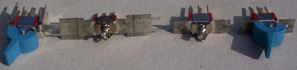
The switches were not hard to find. You can buy ten 7101 switches with blue levers from Electronic Parts for Less for only US$4.99 total. The sides which are meant to be soldered to the PCB can be bent out and holes drilled, so that they can be mounted like in the original instructions.
I bought the five 7108 switches from eBay, but these were of the rocker type. You can also buy these switches from Electronics From Golden O or Mike's Tools and Stuff. I have ordered replacement levers from Switches Plus Components Australia for AU$0.88 each (including GST). They also have 7108 switches, but these cost AU$17.60 each (including GST). They don't have the 7108J2CQE2 (black lever) and 7108J2CQE3 (red lever), but you could try other switches, e.g., 7108J2V2BE2 and 7108J2V2BE3. These are like the 7101 switches from Electronics Parts for Less. There is a AU$22 minimum order with Switches Plus, so I have plenty of spares for sale. The shipping cost is AU$13.20.
I have made up a part list and an order list for EDUC-8 builders. These files don't display correctly in browsers due to the tabs I used. Use Wordpad or CWordpad in Windows to view and print these files. I used the Australian versions of RS Components and Farnell for some of the other components. These two companies operate worldwide, so you should be able to order from your home country equivalent. I also used Dick Smith in Australia for all the resistors and some other components. You should be able find these parts from your local electronics store, Unicorn Electronics, RS Components or Farnell.
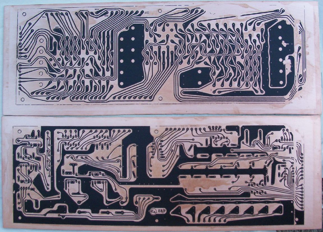
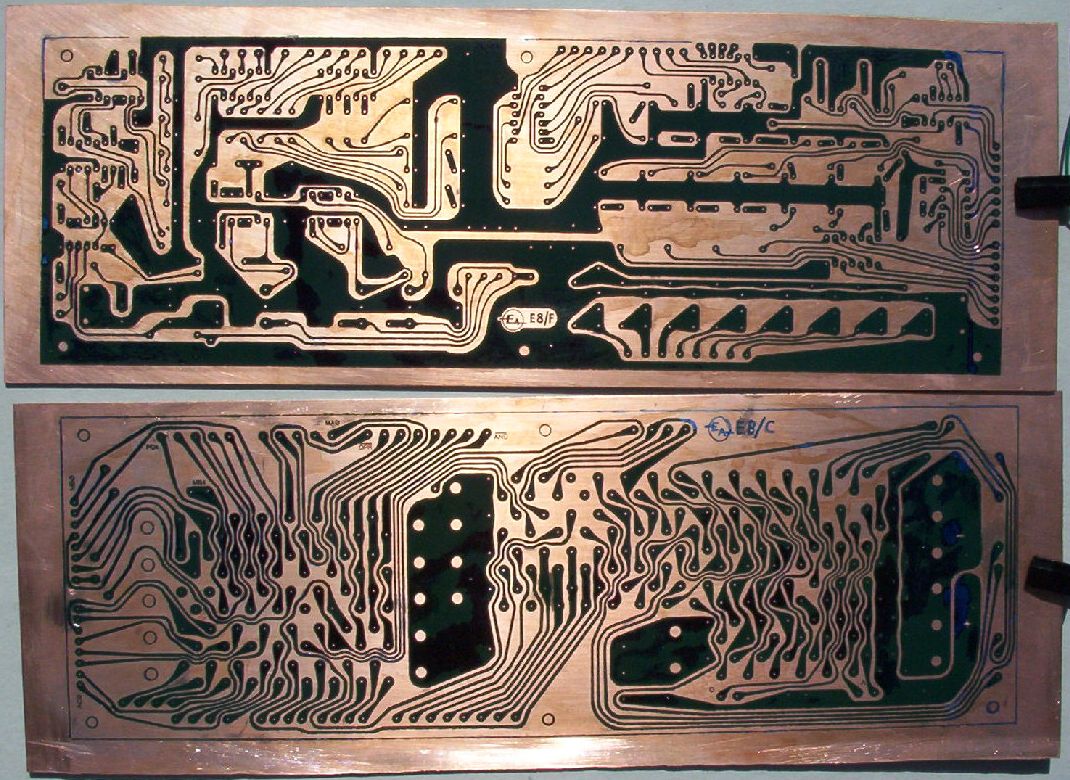
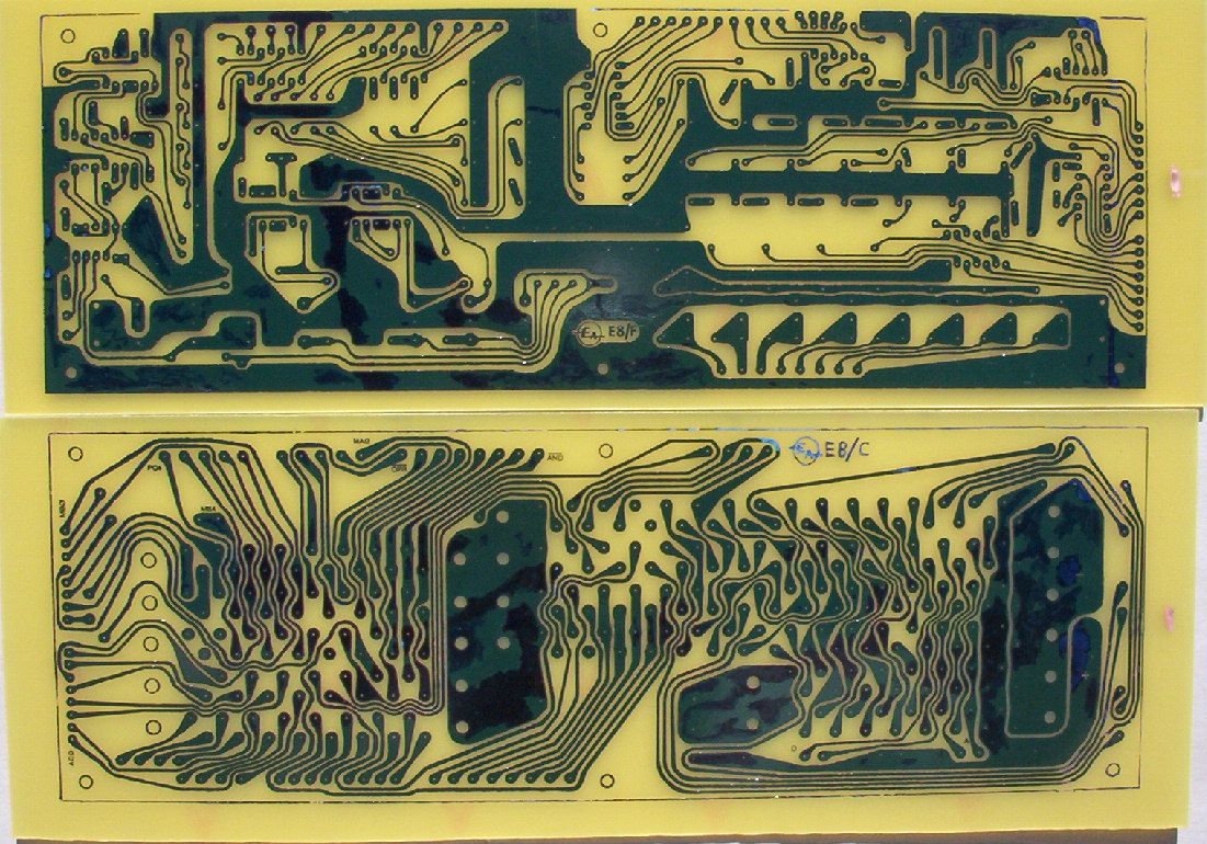
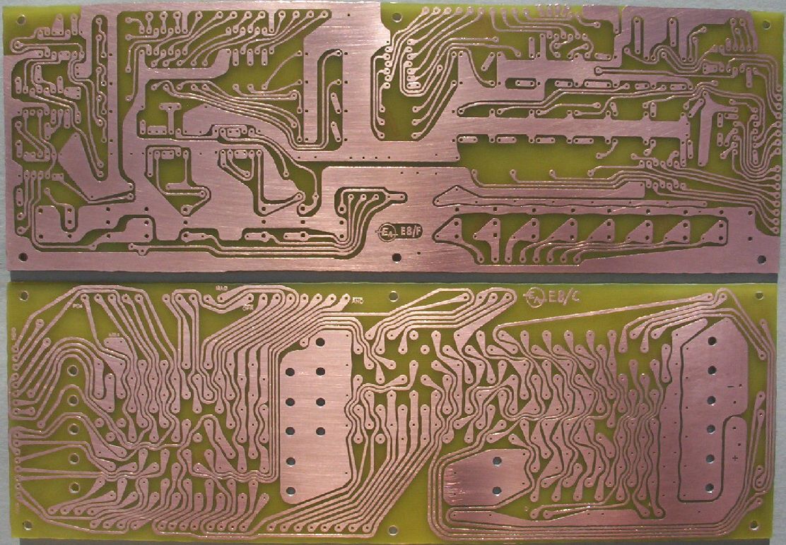
I have now given up on RCS Design providing the PCB boards and have decided to make them myself. Unfortunately, Silicon Chip, the owners of Electronics Australia, do not have the original artwork. However, the artwork is shown in grey in the component placement diagrams. I scan these at 600 DPI and then import them into my QuickSilver (Interleaf) word processor. Using the Create Poly command, I can retrace the artwork. I will be making this artwork available for free once I have finished drawing them. I have completed the front panel board (E8/F) and I'm now working on the connector board (E8/C).
This is a lot of work, but it also allows me to solve another problem, that of finding suitable connectors. Enlarging the connector artwork horizontally by 4% will allow me to use the 0.156" (3.96 mm) connectors I already have! I bought 143 of these connectors in a lot, so I have plenty of spares to sell to anyone who wants them. These connectors don't have side lobes and are 18-way/36-pin. Thus, they still need to be modified in the same way as the Micro-Plastics connectors.
|
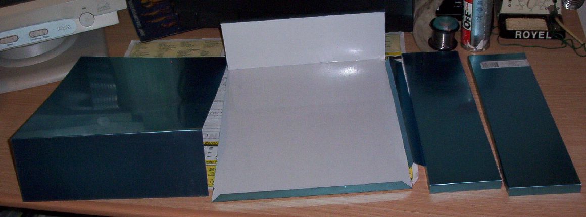
Case parts |
24 Jan. 2007. The power supply and rear connectors are complete and working! On turn on the power supply measures 5.39 V with no load, increasing to 5.43 V with time. This is as expected (5.3 to 5.4 V). With a 500 mA load, the voltage should drop down to about 5.12 V.
 |
Putting together the power supply. The transformer and bridge rectifier are next to the fume extractor. The control circuit is on the printer next to a power cable. On the table the cables to the DIN connector are being attached. |
I used a breadboard for the control circuit, instead of a tag-strip as Dick Smith did not have tagstrips. The layout worked out quite well. I later found out that Jaycar has suitable tagstrips. The original design specified a TT800, BFS92, or AY9139 equivalent PNP medium power transistor. An equivalent is the 2N4033 in a TO-39 case, the same as used originally. However, Unicorn sent me a TN4033 which uses a TO-237 case. This is similar to the common TO-92 case, except that a short metal strip sticks out from the top. I used a strip of aluminium left over from the case to make a heatsink for this. This was bent into a circular shape, with the ends being clipped onto the top of the transistor. You can download a pdf file of the circuit pattern I used here. The grid pattern is 15 by 16, using 0.1" spacing. The board dimensions are 47 mm x 45 mm. I used a small Dick Smith prototype board. I'm going to use the small board that was left over for the two extra LEDs on the front panel.
 |
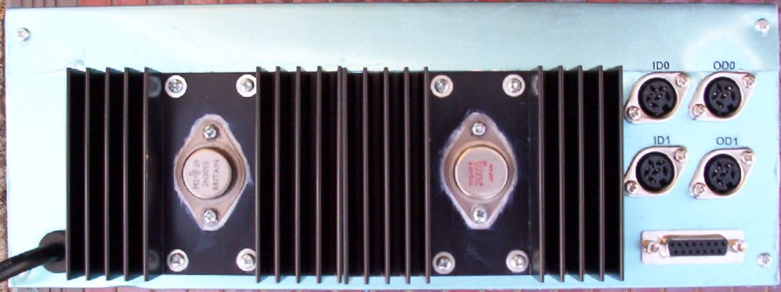
Power supply. From right to left, transformer, bridge rectifier, reservoir capacitor, control circuit and DIN connectors. |
Unicorn Electronics gave me two different 2N3055 transistors, a TI one from Britain and a Toshiba one from Japan. Hopefully, they'll share the load equally. One change I made to the original design is that I have separated the 16 pin connector in the original design into a DIN6 ID0 (input device zero) connector and a 15 pin D-connector for the switch register, external load address and deposit signals. One reason I did this is the original 16 pin connector is no longer available. This connector was originally designed so that EDUC-8 could read data from a punched tape reader. By separating the connectors, I can have two standard input devices (instead of just one). The 15-pin connector can be connected to a boot ROM, e.g., two 256x4 ROMs, which could allow it to load programs, for example to read and write programs to cassette tapes. The connections for the 15-pin connector are
1: SR0 9: GND
2: SR1 10: GND
3: SR2 11: GND
4: SR3 12: LA_
5: SR4 13: DEP_
6: SR5 14: VCC
7: SR6 15: VCC
8: SR7
 |
Rear of case |
I used custom made decals to make the labels for the DIN connectors. This was done using decal paper and my laser printer.
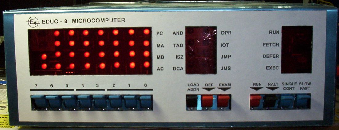
26 January 2007. The front panel artwork has been done. You can download the artwork from here. I made this using a photo of the front panel and Interleaf. The photo is imported into an Interleaf document, properly sized, and from which I recreate all the text, symbols and boxes.
The big job was in making the windows in the cover. First I printed the artwork on a piece of paper and cut out the windows with a sharp knife. The artwork was temporarily attached to the cover with Tamiya masking tape. With a sharp knife I traced out the windows onto the cover. The artwork was removed. As the aluminimum is covered in clear blue plastic, this was peeled off from the windows. I did not have a proper tool, so every 3.5 mm I would drill a hole with a 5/32" drill near the edge of the windows. To help with this, I first marked out the positions of the holes, and then used a punch to mark the position of each hole. The punch marks helps guide the drill, otherwise it moves all over the place. Some of the holes did not overlap, so I used a hacksaw blade to cutaway the aluminium between the holes. The centre piece was removed. To remove the rough edges, I used various files and plenty of elbow grease to make a nice square window. This had to repeated six times for each window!
The back of the artwork was brushed with glue and attached to the cover. The inside edges of the holes were painted matt black. The back of the cover was brushed with glue and clear red cellophane attached to the windows for the various LEDs.
 |
Front panel artwork attached to case cover. |
4 Feb. 2007. I have started making the Front Panel and Connector PCBs. I'm using the Toner Transfer System. I thought this would be easy to produce the mask, but its not. The system works by transferring the toner from a laser printer onto the board. I thought all you needed to do was print the mask on the TTS paper and then iron it on. However, that is just two of the many steps required. You also need to blast the toner on the TTS paper with a heat gun, determine the correct temperature for your iron, soak the board in water to remove the paper, and then use Green TRF film to seal the toner. I didn't know about the Green TRF film, and the Australian store I bought the TTS paper from didn't have it in stock. I thus had to expensively order some in from the US.
The TTS paper is also in an inconveniant Letter size (279x216 mm), while the front panel and connector boards are 283 mm wide. A4 size paper (297x210 mm) would have been perfect. I converted the TTS paper to A4 length by taping an additional 18 mm to the bottom of a page. Unfortunately, the printing was a bit light along the join line. Blasting with the heat gun also caused the paper to separate from the tape. You can see the results below.
 |
Boards after transferring toner. |
The middle of the boards are excellent. The right part of the boards suffers from the additional length added to the paper and the left part of the board suffers from smear to the left of the tracks. I ironed from right to left. The paper might have shrunk during this, causing the smudging. Where toner didn't transfer, I am going to use a printed circuit marker pen to fill in the gaps.
While I'm waiting for the Green TRF film to arrive, I'm doing the artwork for the main PCB's. At the same time, I'm expanding the edge connectors tracks by 4%, so that they will fit the 0.156" connectors I'm using. I finished the Timer Board yesterday. Each board takes me about two days to do. I only have another five main boards to go, plus the Display and Keypad boards!
I have also scanned my EDUC-8 articles for safe keeping. My paper copies are starting to yellow, so having them on a CD should make them last longer. The scans were done at 400DPI and in colour. There are 79 pages in 13 articles from August 1974 to August 1975. Each page is about 3MB in size, and 217MB altogether. The articles are
Aug. 1974: Build your own digital computer!
Sep. 1974: Our do-it-yourself computer: how it works
Oct. 1974: Our EDUC-8 computer: starting construction
Nov. 1974: Building our computer: three more sections
Dec. 1974: The EDUC-8 computer: getting it going - at last!
Jan. 1975: EDUC-8: adding the input/output interface
Feb. 1975: Programming your EDUC-8 microcomputer
Mar. 1975: Interfacing EDUC-8 with punched paper tape
Apr. 1975: Interfacing EDUC-8 with a Philips 60SR printer unit
May 1975: A full ASCII-type input keyboard for EDUC-8
June 1975: Teaching your EDUC-8 to play a melody
July 1975: Interfacing EDUC-8 to teleprinters & mag. tape
Aug. 1975: Interfacing a Burroughs self-scan display panel to your EDUC-8
20 Feb. 2007. Unfortunately, I've been busy going to a local conference and reviewing my student's PhD thesis, so I have not been able to get much done. This week I've done some work on the PCBs. The Green TRF arrived. This is used to seal the toner. I cut out a sheet, placed the dull side against the PCB, placed a piece of paper on top, set the iron to mid-way, and ironed as hard as I could for 30 seconds. I repeated this a second time. Unfortunately, not all the Green TRF transferred, so I had to fill in any missing patches with a printed circuit marker (which comes out in blue). I also used the marker to fill in any missing tracks.
 |
Boards aftter transfer of Green TRF and patching with marker pen. |
For the Connector Board, I bought a GBC Creative A4 Laminator from K-Mart. Unfortunately, this did not have enought heat to transfer the Green TRF. I did three applications of the iron, but this was too much as some of Green TRF stuck to the copper, while not all transferring to the toner!
 |
Etching the Front Panel Board. |
The next step was to etch the boards. I'm using an etching tank. After waiting half an hour for the water to warm up to 50 C, I added 440 g of Ammonium Perchlorate. This dissolved very quickly. The board went in, just fitting lengthwise to the 300 mm depth of the tank. As the copper etched, the solution goes from clear to blue, from the copper salts. After about 7 minutes, a small patch of copper was etched away. In about 30 seconds, all the visible copper was gone. I pulled the board out and gave it a wash. The second board seemed to take about 5 minutes, perhaps due to the solution warming up to a higher temperature.
 |
Boards etched. |
19 Mar. 2007. Its been nearly one month since my last update. During that time I have drilled the front and connector boards, nearly completed the front board, and modified the switches.
To drill the boards, I used a drill press I bought on eBay where a standard drill bolts in. Our drill is very loud, even with earplugs and earmuffs! I used a 0.8 mm tungsten carbide drill bit for the wire links, resistors, capacitors, edge connector pins and integrated circuits (ICs to us electronic engineers, microchips to Hollywood). For the light emitting diodes (LED) I used a 1.0 mm bit. For the first LED hole I used a 0.8 mm, followed by 1.0 mm. The end of the 1.00 mm drill bit jammed in the 0.8 mm hole and broke the tip of the bit off! I learned from my brother that this is a common problem when drilling. Its better to not drill in two stages. I did not have a spare 1.0 mm bit, but fortunately the break was clean. I just had to press a little harder with the 1.0 mm bit. I also used the 1.0 mm for the wire connectors around the edge of the board.
For the larger holes on the corners and the edge connector mounts I used a 1/8" (3.175 mm) drill bit so that the 3 mm screws would fit through. For the switches I used a 1.2 mm tungsten carbide bit. I initially used a 1.2 mm bit for the mounting holes of the switches bracket. No screws would fit this, so I enlarged the hole to 1/8". However, the head of a 3 mm screw would overlap a track next to it, causing a short. I got some 2.5 mm screws which avoided this problem. For this size screw a 7/64" (2.778 mm) bit should be used to drill the hole.
After drilling the holes, I then used a hacksaw to cut the boards to size. I found this to be a lot of work. I then used a steel wool brush from the kitchen to rub away the toner mask. I later discovered three holes that needed to be drilled. Its easy to miss a hole! The final step to prepare the boards is to spray them in Servisol PCB Laquer that I bought from Jaycar. This prevents the copper from corroding. Soldering is no problem, as the hot solder easily melts the laquer. As you can see, making a PCB is no easy task!
 |
Boards after drilling and cleaning. |
The next step was to solder in the components. I started with the front panel board. The components are added in increasing height, starting with the links, resistors, IC's, capacitors and then LEDs.
 |
Front panel board with most components loaded. |
The next thing to do was to modify the switches. The switches I bought had side mounted brackets that solder directly to the board. The original design had flat brackets, but these are no longer available with solder pins, only with solder tabs. First step was to remove the levers. I did this by pushing the lever out of one hole in its bracket, holding it in position, and then using a screw driver to push the lever out of the other hole.
Step 2 was to flatten the brackets. This was a complicated process of first levering the bracket out slighty with a screw driver, flatting the sides with a plier, partially flattening the top of the bracket with pointy nose pliers, hammering flat the bracket with a small hammer and a slege hammer acting as an anvil, adjusting the bracket with a plier and then repeating all this for the other side and fourteen other switches!
While working out this procedure, I managed to break a pin loose from a 7108 switch. Ironically, I had no spare 7108's, but I had spare 7101's, and the side I broke was the one that was used. Had I broke the other side or broke a 7101 (which was twice as likely), I would have been fine. Talk about Murphy's law! I superglued the pin back, but unfortunately, the connection did not work. With nothing to lose, I decided to take the switch apart, prying loose the metal sides. The switch is actually pretty simple inside. There's a lever which connects the middle pin to either side of the outer pins. By swapping this lever around, I could make the good side active. While hammering the sides to get them back in place, the whole side of the switch broke away! To fix this, I superglued it back on, and then superglued the metal sides. Both sides now work, but I will only use the good side for the computer.
Step 3 is to cut the brackets to shape. I first drew lines on the bracket that were 30 mm apart. I tried to use an old tin snips from our garage, but this was very badly worn and out of shape. I managed to make a short cut, but had to finish it with a hack saw, which was not very easy. I threw the old tin snips in the bin and bnought a new tin snip which worked perfectly. The little edges that were left over were cut of with sprue cutters that I got from the Airfix Classic Club membership! The wire cutters I got from Dick Smith were not up to the task.
Step 4 was to drill the holes. I first marked these 24 mm apart with a pencil. I then used a punch to inititally mark the bracket. The holes were then drilled with a 3/32" (2.381 mm) drill bit, so that 2 mm screws could be used. Finally the back the of the screws were filed down to remove any burrs. The corners of the brackets were filed down as well, to prevent myself from being accidently cut. As I previously didn't anticipate the 2 mm screws, I bought some 2 mm screws, washers and nuts from RS Australia.
The final step was to reinsert the levers, which is pretty easy. As you can see, nothing is easy with this computer!
 |
From left to right, original switch, bracket flattened, bracket cut, completed switch. |
I've also been buying some tools so I that making the PCB's is a bit easier. First of all, I bought a paper guillotine to cut the boards. The one I chose is the Ledah 405 A4 Guillotine from Thinkgroup. This is about three times what you pay for a cheap guillotine, but at least you won't accidently cut your fingers off. This guillotine can cut up to 20 pages, which I figured should be enough to cut a 1.6 mm thick PCB.
I used the guillotine to cut the remaining PCB boards, all nine of them. Doing a long 305 mm cut was easy in the beginning, but got very hard near the end, even with a curved blade. Also, the board tends to pull to the right, so that you overcut the board. Adjusting the end of the board a little to the left compensates for this. Even with these disadvantages, I managed to cut all the boards in less than half an hour, much faster and easier than the old method with a hack saw.
The latest item I have bought is a GBC Heatseal H210 A4 Laminator from Nexus Australia. The laminator will be used to transfer the toner and seal the PCB. This is the laminator recommended by Pulsar, who make the toner paper. I tried the laminator with some spare TTS paper and board, but it did not work! The laminator was set at its maximum temperature, I tried the board up and down, nothing. The toner would not stick. After a while, I tried putting the board repeatedly through. This seemed to do the trick and the toner stuck very well. The Green TRF seal also stuck very well. So, I'm all set to make the rest of boards, once I get all the artwork done.
As to the artwork, while waiting for various things, I have started work on the second computer board, the E8/D or decoder board. I have also contacted a local company, A Class Metal Finishes, who said they can gold plate the edge connectors of the PCB's. This is important, as one of the problems reported with the EDUC-8 is intermittant connections with the edge connectors if they are not plated correctly.
13 Apr. 2007. Another big update. This time I have finally completed the first part of construction!
The first thing I did was make a bracket for mounting the switches. I used some spare 0.5 mm thick aluminium sheet, 30 mm wide by 282 mm long. I used the PCB to mark out the locations for the holes for the switches and screw holes. The ends were bent into a bracket 10 mm high and 10 mm wide. I then did the tedious task of making the holes. Six small holes were drilled around the perimeter of the rectangular hole. The middle was cut out. Using a small round and triangular file, the rectangular hole was shaped. This was repeated 13 times! Two small holes for each switch were drilled, using a 3/32" (2.38 mm) drill bit. I used the drill press for this task. In the top left corner, I cut part of the bracket away to make room for the 47 µF tantalum capacitor.
The bracket was screwed in place and the switches carefully inserted. I then carefully screwed the switches in place using 2 mm screws, washers and nuts. This was sometimes a tricky operation. It might have been easier to screw the switches to the bracket first, and then attach the bracket. After all the switches were screwed in, I realised that the bottom left and right corners of the bracket would interfere with the front spacers. I removed the bracket and switches as one unit, used a small round file to make clearance, and reattached the bracket and switches. The switches were then soldered in.
 |
Switch bracket. The bottom left and right corners need to be filed to make room for the front spacers. |
The small daughter board for the PC7 and MA7 LEDs was made up and attached to the front board. I used small strips of tin cut from a Nestlé Quick can to make the bracket. The bracket was soldered to the +5 V rail along the top of the board. A small drop of superglue under the board was used to attach it to a 7405 IC underneath.
Finally, I soldered in solder pins for the switch register, external deposit and external load address. I later realised that I should have not soldered in the pins for the switch register. The pins should be soldered to the connector board, as this allows easier access to the cable used to connect to the rear connector. This completed the front panel board!
The Electronics Australia article says to test the LEDs after completion of the first section. However, if there is a bad LED, IC or resistor, it would be a big job to unsolder all the links between the front and connector boards, in order to replace the broken part. Thus, I tested the front board as soon as it was completed. As the laquer had insulated the contacts to the LEDs, I wiped these clean with some white spirits. The two LEDs on the daughter board and the instruction and status LEDs are normally dark, with the rest on. On power up, the LEDs lighted up correctly. Shorting each input to ground, I then tested each LED. All worked correctly!
 |
Testing the LEDs. |
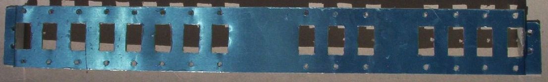
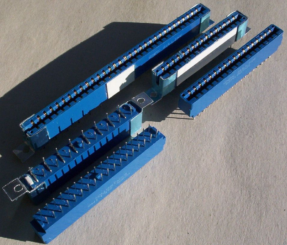
The next big task was to modify the connectors for the connector board. What I had were 18 way double row connectors without side mounts. What I needed were 16 and 32 way single row connectors with side mounts. Including the extender board, I needed five 32 way connectors, one of them closed ended for the timer board, the other four open ended on one end, and eight 16 way connectors, all of them open ended on one end. Using sixteen 18 way connectors, I would make the thirteen connectors (equivalent to eighteen 16 way connectors).
The first tedious task was to convert from double row to single row. The connector board also had the pins going alternatively up and down. To achieve this, I would alternatively cut off pins from the top row and alternatively bend up pins from the bottom row so that the bent bottom row pins would lie next to the remaining top row pins. These bent bottom row pins were then soldered to the top row pins. A total of 16x9 = 144 pins had to be soldered.
The next tedious task was to cut the connectors to the right number of connections. I used a razor saw that is used by modellers. The plastic is fairly hard, which made cutting the connectors difficult. I would first scratch a line into the plastic sides to aid in cutting the connectors. For each 32 way connector, I would cut off the end of one 18 way connector, and cut off four pins from the other 18 way connector. For four of the connectors, I would open up one end using the razor saw and a sharp modellers knife.
The two connectors would then be inserted into the connector board. I would then insert a spare piece of PCB into the connector and remove the connectors with the PCB still inserted. The connectors would be adjusted and temporarily test fitted back into the connector board, to make sure the spacing was correct. I cut two pieces of 0.5 mm thick plastic card, of size 14x20 mm. Superglue was applied to the connector, 10 mm from each side of the join line, and on one side of the plastic card. The card was attached and repeated for the other side. This makes for a surprisingly very strong join.
To make the 16 way connectors, I would cut off one end, and then cut off two pins. The end would be reattached with superglue. Using the spare 4 way and 2 way connectors left over, I made two 16 way connectors. The 4 way connectors were used at the ends. One connector had four 2 way connectors in the middle, while the other connector used a 4 way and two 2 way connectors in the middle. The connectors were joined using the same technique as for the 32 way connectors, except that a longer piece of plastic card was used. Again, the connector is surprisingly very strong and level. I used the left-over pins as this was actually easier than cutting off new pins.
Using the razor saw was very difficult. I would recommend buying a diamond cutting wheel from RS Electronics (part number 472-3038). This should make the task much easier.
The final tedious task was to make the side mounts. My connectors did not have any. I used spare 0.5 mm aluminium sheet. These were cut into 23x29 mm squares. The 29 mm length was marked at 10 and 19 mm (giving 10, 9 and 10 mm sections). The 23 mm length was marked at 8 and 9.5 mm (giving 8, 1.5 and 13.5 mm sections). In the 9x13.5 mm section, a 3x8 mm section was cut out of 12 of the side mounts, to make room for the PCB to slide through.
Two corners of 10x9.5 mm area were cut off. The 9 mm wide tab was bent up at the 8 mm line. The 10 mm wide tabs were bent at the 10 an 19 mm lines. Using a connector and the connector board as a guide, I marked out a hole at the bottom of the side mounts. These were then drilled. A tricky operation, as I had to drill from the bottom of the mount. I held the side mount onto a connector to help with this.
While fitting the side mounts to the connectors, I found that it was easier if the square corners of the connectors were filed down into a round corner. For fitting the side mounts (all 26 of them), I first put the connector into the connector baord. Usually, I had to adjust the side mount, so that it would fit tightly to the connector. I applied lots of superglue to the inside of the side mount and the end of the connector. This made for a very strong join.
With the side mounts all on, we could finally bolt the connectors in place. However, with the rounded corners, the side mounts had moved inwards. Thus, the side mount holes were not in the correct position. The new position of the hole was marked out on the side mount. A small round file was used to make the hole in the right position.
Now we could finally mount the connectors in place and solder the 240 pins to the board! I have lots of spare 0.156" 18 way connectors for sale (only AU$1 each), but you might want to buy the same connectors, but with side mounts from Jamma Boards for US$1.75 each.
 |
Connectors, before and after modification. |
For those with 0.150" (3.81 mm) original EDUC-8 boards, you could cut these 0.156" connectors down to 0.150". Using the diamond cutting tool, you can cut off two ways at a time, keeping each piece numbered, so that you can put them back together in the right order. The pins in the 2 way connector will be 0.006" (0.15 mm) further apart, while the distance between the 2 way connectors will be 0.006" (0.15 mm) closer together. There should be enough tolerance so that these small variations should not matter. Using the techniques I described above, the 2 way connectors can be joined together to make 16 and 32 way connectors. Its not a trivial amount of work, but its a lot cheaper than having to custom order 0.150" connectors, as I could not find any off-the-shelf source of 0.150" connectors with solder pins.
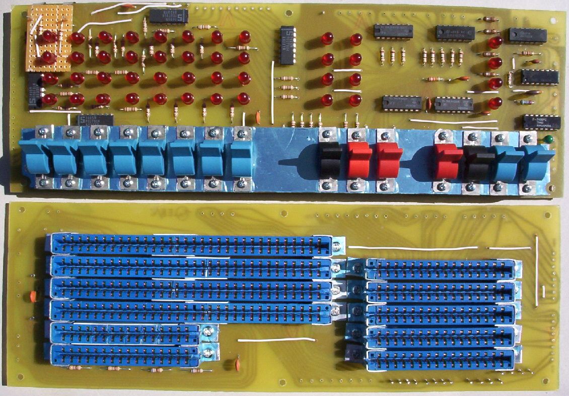 |
Completed front and connector boards. |
Before joining the two boards together, wires for +5 V and GND were soldered from the solder pins from the connector to the front board. I also soldered a short wire to the External Deposit pin near the middle of the front board. I should have made this wire longer, so that it reached the end of the switch register cable inside the case.
 |
Power lines between front and connector boards. |
The two boards were then connected together via spacers. The tedious task of then soldering link wires between two boards then had to be done. The wires between the bottom and sides of the board are fairly straight forward. However, one has to be careful in wiring along the top edge, as longer insulated wires are needed, along with pins not being in the same order between the boards. This is not a good design, as fixing a fault would need the removal of nearly all the link wires. An old EDUC-8 solved this problem by using long strips of ribbon cable between the boards.
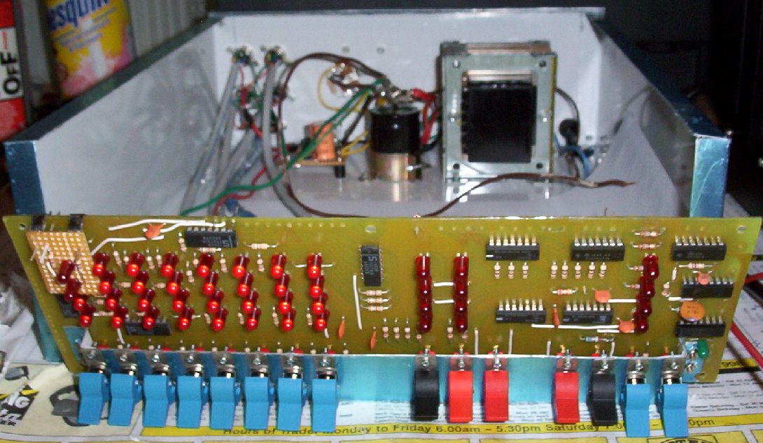
While fitting the two boards into the case, I noticed a problem. I had installed the sides of the case back to front, so that the front lip was shorter than it was supposed to be. The long lip was at the back! This meant I could not mount the boards, as the front lip was too short. I solved the problem by attaching small pieces of alumuninum sheet, to extend the front lip in the four corners. I used some counter sunk screws to hold these in place. I had tried superglue, but it did not work.
The next step was to solder the cables to the rear solder pins of the connector board. The switch register cable was soldered to the front board, as I had incorrectly soldered mounting pins on this board, instead of the connector board. I also had to solder short leads between the switch register cable and the external deposit wire and load address pin on the front board. The power and ground wires were also soldered to the connector board.
 |
Wiring rear connectors and power to boards. You can also see the tabs I added to the front of the case. |
I could finally now mount the two boards into the case. I used 30 mm long countersunk screws. The instructions recommend 1" (25.4 mm) long screws. The 15 mm spacers I had bought were too short. I cut off 5 mm from some spare spacers to make a 20 mm long spacer. The front boards also now added rigidity to the case, which was a bit flimsy from using 0.5 mm thick aluminium.
 |
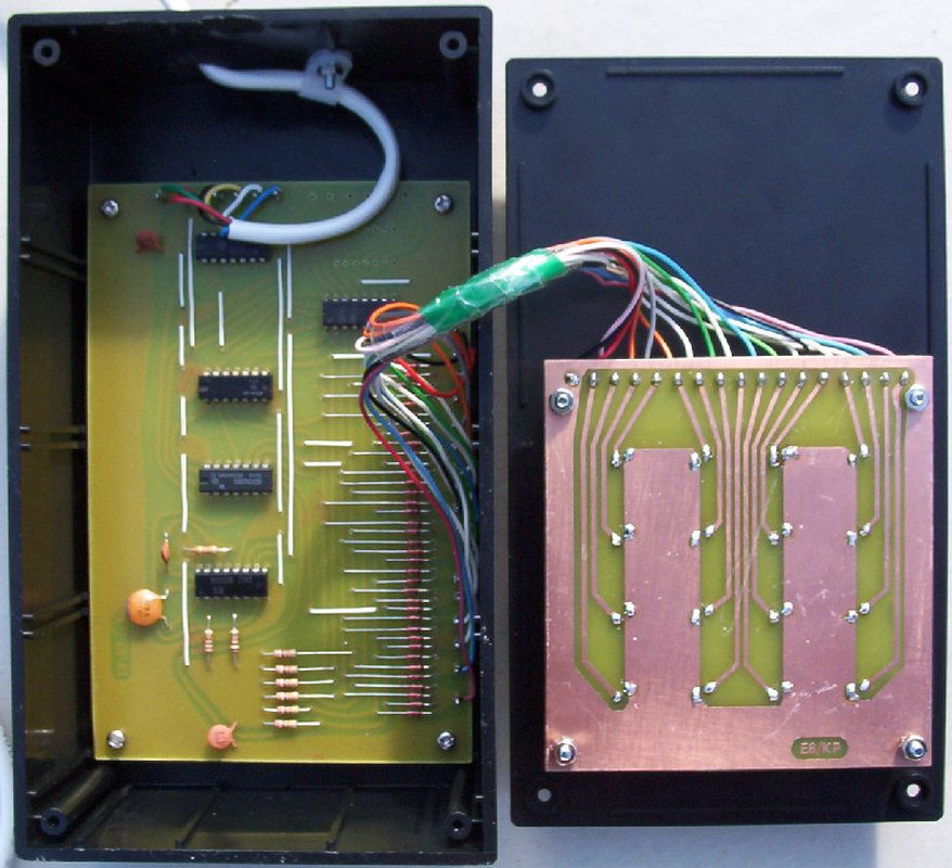
Boards installed in case. Connector view. |
With the board finally mounted, I powered the computer up, to make sure all the LEDs were working. I noticed that the +5 V mounts for the daughter board was touching the case lid. To prevent shorts to case ground, I put some insulating tape on the bracket.
 |
Boards installed in case. Front view. |
For the case lid, I made the right most hole for the switches a little larger to the left. This allowed the case lid to sit a little better. Finally, I drilled holes into the case lid, to match the smaller holes in the case I had previously drilled.
 |
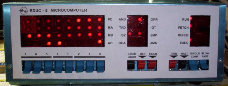
First section completed and working. |
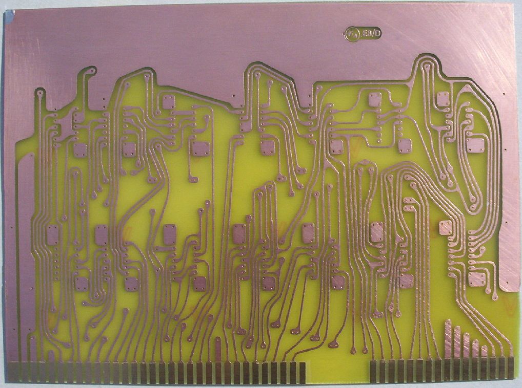
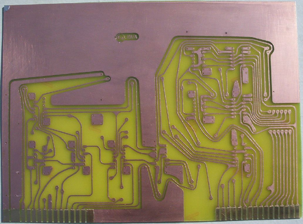
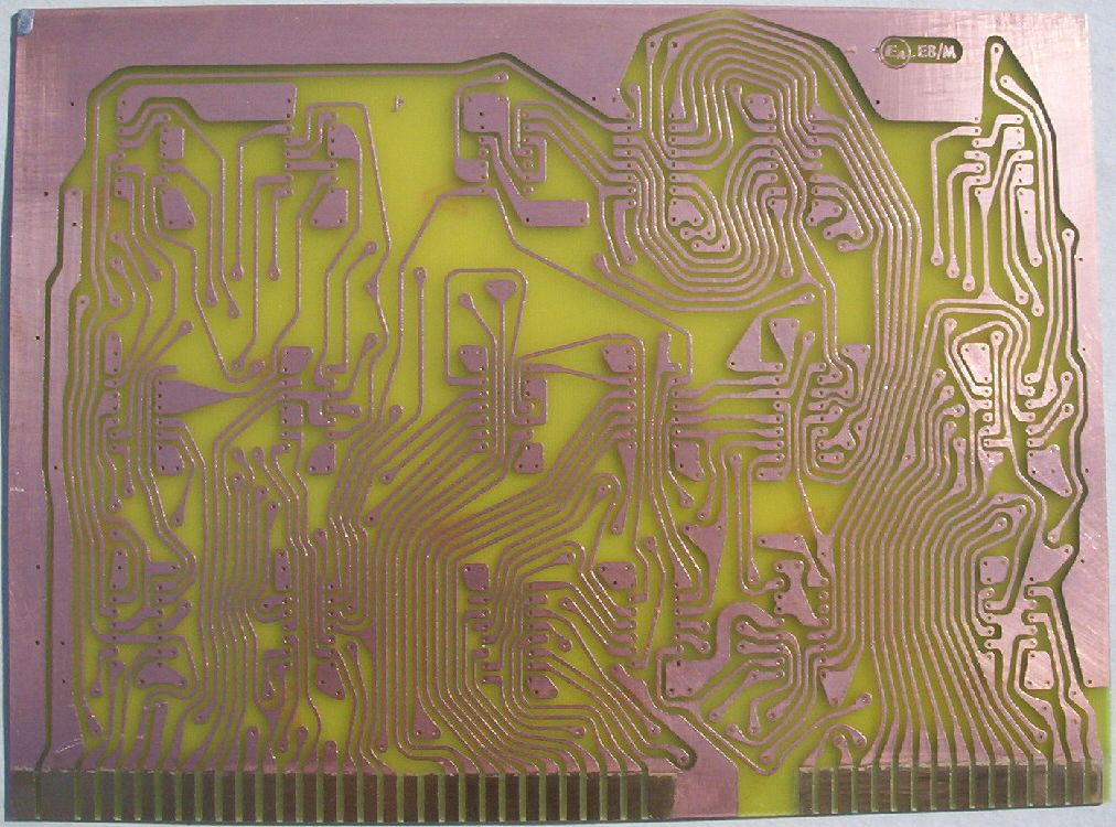
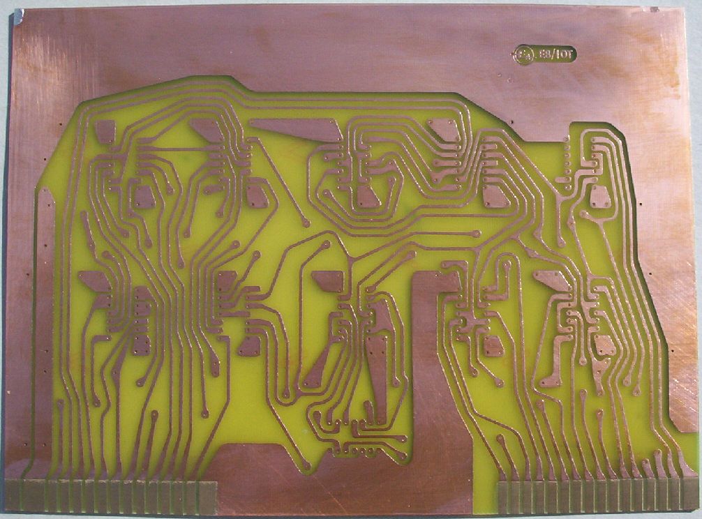
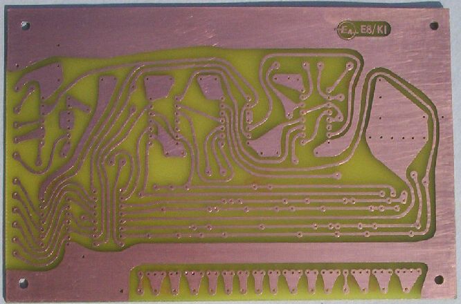
My next update may not be for quite a while. I have to do the PCB artwork for all the six main boards, extender board, and three smaller peripheral boards. I've already done the timer board and started on the decoder board. I intend to make all the next boards in one batch.
26 June 2007. A short update. The artwork is coming along. Boards still to do are E8IOT, E8X and the three interface boards. Thanks to Garry Page's EDUC-8 blog, I have discovered that a 74 series equivalent for the 9001 does exist, the 74105. It has the same pinout as the 9001. Its available for $1.99 from Unicorn Electronics.
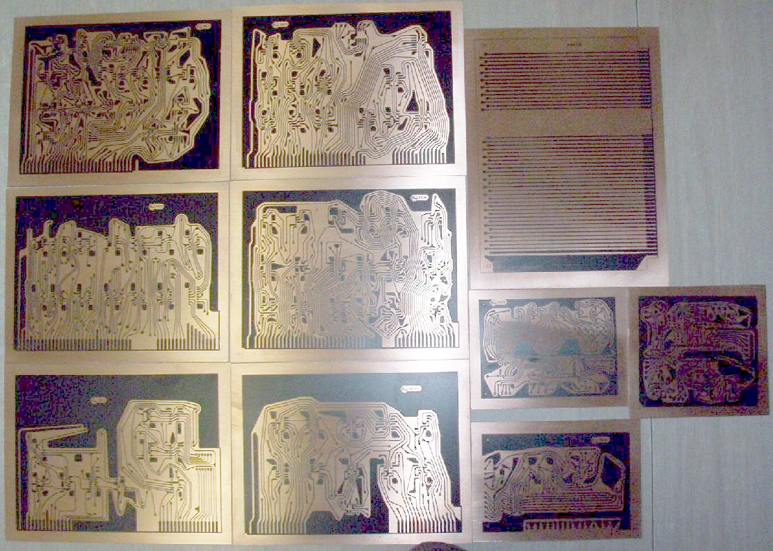
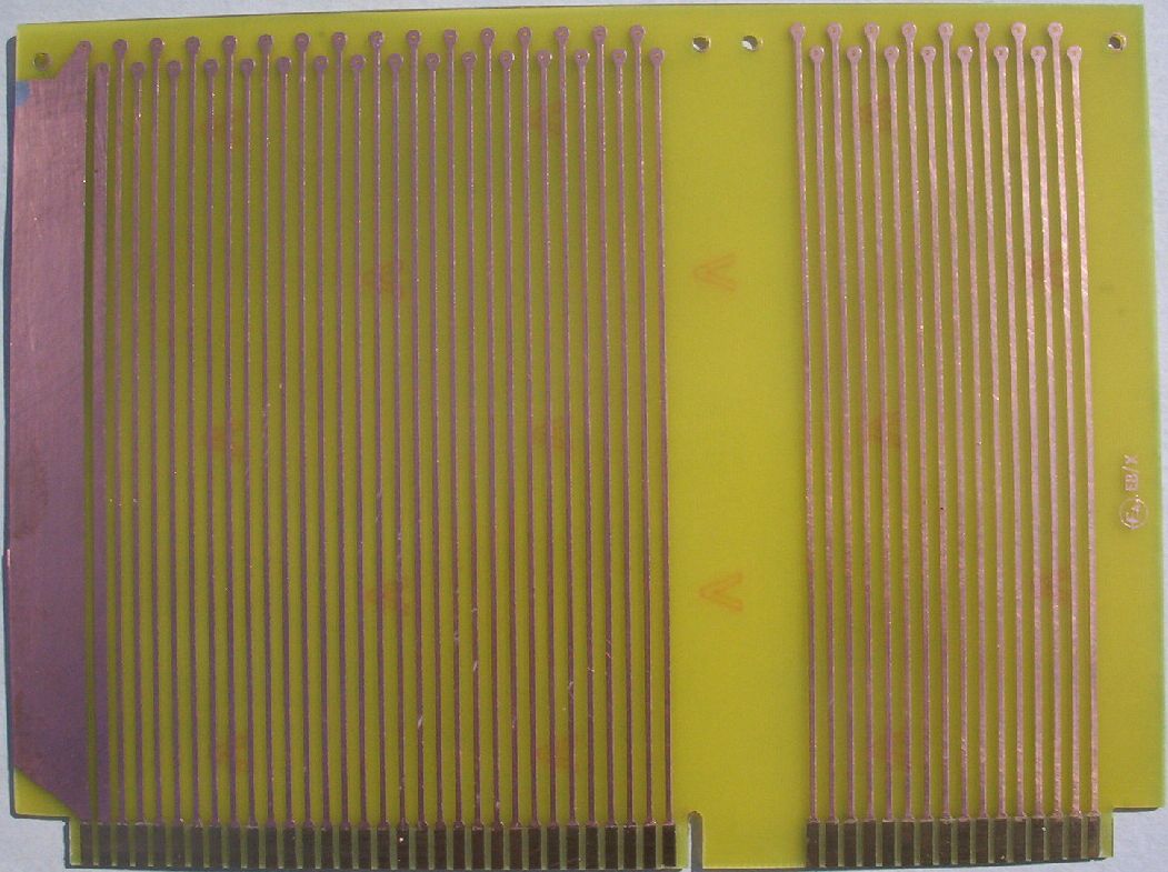
3 July 2007. I've finished laying out the boards! You can download all the printed circuit patterns from the resources section below. I am making these patterns available for free. All I ask is that they are for personal use only. Hopefully the patterns in the Electronics Australia articles do not have any errors and that I myself did not make any errors in copying them. The patterns are in postscript format. You will need GSview to view and print the files. Please don't ask me to provide the patterns in another format, as I won't be doing this. All the patterns are mirror imaged. Thus, you can print directly to Toner Transfer System or Press-N-Peel paper. You can also print to clear film, with the ink side against the PCB.
I've printed nine pages on Toner Transfer Paper. I first used a yellow paper. I also used some new blue paper, which seems to be a little stiffer. The first try with the blue paper, the paper jammed, causing a loss of paper. The second try, I was careful to gently push the paper in. This worked fine. Next step is to actually make the boards!
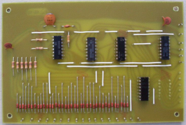
7 August 2007. All the boards have been made! I list the steps below.
 |
Boards after transferring toner. |
 |
 |
 |
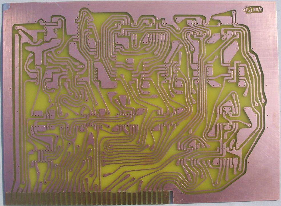
| E8/T Timing Board | E8/D Decoder Board | E8/A Accumulator Board |
 |
 |
 |
| E8/P Program Counter & Adder Board | E8/M 256-Word Memory Board | E8/IOT IOT Interface Board |
 |
 |
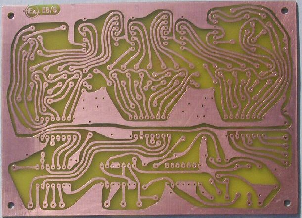 |
| E8/X Extender Board | E8/KI Simple Input Keyboard Board | E8/S Octal Display Unit Board |
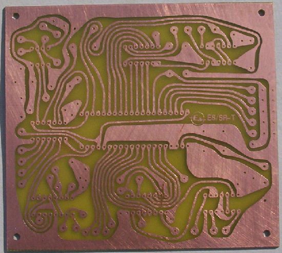 |
E8/SR-T Asynchronous Serial Interface Board |
So, I have now reached the stage where I can now finish building the computer. Cross my fingers that the boards will work!
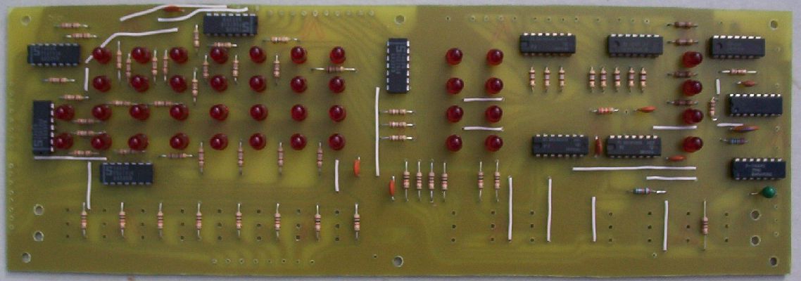
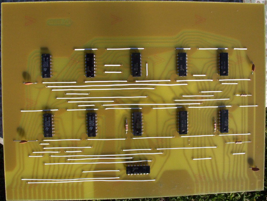
10 August 2007. The second section is completed and working! I spent this week assembling the Timer Board (E8/T), Decoder Board (E8/D), and Accumulator Board (E8/A). The instructions for this are described in the November 1974 issue of Electronics Australia (EA). The first task for each board is inserting the wire links. I used insulated solid core wire that I found in my wire bin. I think this wire was used in the telephone system. Anyway, what a tedious job it is soldering all those wire links! There's a huge number of them. The boards were designed to be single sided to reduce cost.
 |
 |
 |
| E8/T | E8/D | E8/A |
For the IC's I used a wide variety from a number of sources. They ranged from a TI 5404 from 1969, some Fairchild 9003 (7410) and 9004 (7420) chips from 1974 and other IC's from the late 1970's and early 1980's. I found that the TI chips needed to have their pins rubbed down with sandpaper to remove all the oxidation and gunk that has built up over the years. This was especially true for the chips made in El Salvador. Otherwise, the solder would not stick to the pins.
In order to test the board, I soldered wires from the Switch Register pins at the bottom of the Front Panel Board to the MB pins to the upper left of the board that go to the display LEDs and computer. This allows you to do some basic tests of the eight instructions, as described in the EA article. With the three boards plugged in, I plugged in the computer to power it up, saying "Here goes!". To my relief, it powered up correctly, as shown below.
 |
Power on. The Fetch light is on, the accumulator is random and MB is zero as expected. |
I then tested the eight basic instructions. Everything worked perfectly, with the status and instruction lights lighting in the correct order. The next command to test was CMA (complement accumulator). This uses code 704 where the first and last digit are in octal and the middle digit is quaternary. I tried this with the accumulator cleared, but nothing happened! On powerup, the accumulator contents are random. Trying this in slow mode, you can see the accumulator shifting right, but no inverted data was being input to the left, effectively clearing the accumulator.
Seeing as I had a problem, I built up the Extender Board (E8/X). This just involved soldering in the 16 and 32 pin connectors I had made previously. I plugged the Extender Board into the Decoder slot and checked to see that the CMA signal was working. This signal went low as expected. I then looked at the Accumulator Board, examining the circuit diagram. CMA was getting to the circuit, and the inverter and NAND gate it went to was working. Looking at the schematic more carefully, the serial input to the accumulator shift register was from the A-BUS. The output from the inverter goes to the B-BUS. These two buses are only connected throught Program Counter and Adder Board (E8/P), which hasn't been built yet! I then checked the later issues and found that the next article had a little section saying that CMA won't work correctly as described. So, the computer was working correctly.
The next instructions to test were clear accumulator (CLA or 710) and rotate accumulator left (RAL or 702), which worked fine. I then tried rotate accumulator right (RAR or 722). In this case as E8/P is not connected, zeros should be shifted in from the left. With random data loaded from powerup, nothing was happening! I checked that the RAR signal to the E8/A worked correctly. However, this signal is not used to cause a right shift. The signal T13.RAR is used. This signal goes low when the timer counter is 13 and RAR is high, causing a single right shift.
This signal measured 1.8 V to the three input NAND gate it went to on E8/A. This was stange as normally the signals are close to zero or around 4 V. As this is a dynamic signal, I got out my old cathode ray oscilliscope (CRO). The signal didn't move. I then looked at the E8/D schematic and didn't see it there. I eventually traced the source of T13.RAR to E8/P! So the computer was working correctly. The 1.8 V was due to no signal being connected to the input. Seems that Mr. Rowe did not obviously test his test instructions.
As the tests were completed, I unsoldered the link wires on the front panel board. I also took the opportunity to solder in three jumper wires to SR5, SR6, and SR7. These go to E8/P since Mr. Rowe did not modify the connector board from his original design with a 32 byte memory. Next to do are E8/P and the Memory Board (E8/M).
23 August 2007. The third section is complete and working! This section includes building up the E8/P and E8/M boards, as described in the December 1974 issue of Electronics Australia. These two boards complete the inner workings of the EDUC-8, except for the interface board E8/IOT. Thus, we can run programs, but can't use it for anything, accept controlling the accumulator register (AC) on the front panel.
First up was building the boards. This was similar to the three main boards, except that we had to add PCB pins for the flying leads and solder IC sockets for the two 1Kx1 memory chips. The lead spacing for the memory chips on the PCB is slightly wider than 0.3" (7.62 mm), so the sockets were hard to fit in. It probably would have been better to cut the sockets in half and solder each half in separately. The PCB pins were bent down so that they would not short to any tracks on the above board. I also added labels next to the PCB pins. Flying leads to the LEDs were soldered the front panel board. At the end of these leads I soldered PCB pin sockets and attached a label to the end of the lead. You can download these labels from the Power Supply Circuit Diagram.
While building E8/P I found I was short by two 2.2K resistors. Going back through the parts list, I found the Timing and Control Board parts list incorrectly listed two 2.2K resistors, instead of the correct four. I went down to Dick Smiths to buy the missing 2.2K resistors, along with PCB pin sockets. I have updated the parts list with the correct number of 2.2K resistors.
 |
 |
 |
| E8/P | E8/M | E8/X |
We then set about testing the computer. All the boards were plugged in, flying leads attached, and power applied. The first test passed successfully, i.e., loading the PC register using the LOAD ADDR switch. The second test failed. This is where we examine the RAM contents using the EXAM switch. Loading address 00000000 (I'll be giving binary here) first and pressing EXAM, the PC counter should increment, but it did not. If address 00000001 is loaded, pressing EXAM gave 11111111, instead of 00000010. Similarly, 00000010 gave 11111110, 00000100 gave 11111100, etc. Thus it appeared the adder and carry FF appeared to be doing something, but not correctly.
 |
Inside the EDUC-8. |
The next step was to understand how the adder circuit worked. The design uses the 7480 full-adder. A full adder has the summation output S = A ⊕ B ⊕ CI and carry output CO = A.B + CI.(A+B) where A and B are the two bits being added and CI is the carry input, ⊕ is XOR addition, + is OR addition, and . is AND multiplication. The 7480 has A = A1.A2+AC and B = B1.B2+BC. Both S and S are given as outputs along with CO. In the EDUC-8 design A2 = B1 = 1 (VCC), A1 = B-BUS and B2 = C-BUS so that A = B-BUS+AC and B = C-BUS+BC. The CI input is connected to Q of the carry FF (the 9001), with the CO output connected J and K of the carry FF (effectively making the 9001 a D-FF with negative output).
During the EXAM cycle, the carry FF is set, PC0 (the LSB of the PC register) is connected to the B-BUS, C-BUS is high, AC is low, BC is high, and S is connected to the A-BUS which feeds into the serial input of the PC register. I was initially confused by all the negative logic, thinking that PC was being incremented instead of PC. However, I later realised that if we feed in inverted inputs to A, B and CI, the outputs at S and CO are non-inverted!
One problem with doing the testing is that EXAM can only be used correctly if the computer is set to FAST (500 kHz clock rate). However, the exam and fetch cycles are very similar, with the PC being incremented. Starting at address zero, I managed to load in the AND instruction. Since the PC was not being incremented at address zero, I could repeat this instruction using the RUN key, with single step operation and in slow mode. This would allow me to follow the signals using my two channel CRO.
Using the extender board, the first pin I measured was A1 (pin 2) of the 7480 on E8/P. This should have been high (about 4 V). However, I measured this to be in the low state! That is, B-BUS was being pulled low. I first checked the single open collector NAND gate connected to B-BUS on this board. One input was low as expected. Turning the power off, I then checked if there was a short on the B-BUS, which there wasn't. I then checked E8/M using the extender board. This again had one open collector NAND gate connected to B-BUS. Both inputs to the NAND gate were high! One input was connected to the D-BUS which was expected to be high. The other input went to an inverter. The input to this inverter is T2-9.ISZ. This input should be high, but was at about 1 V. With the power off, I measured only 84 Ω to ground! With the board out, the resistance was greater than 10 MΩ as expected, so the problem was not the inverter. This signal also goes to E8/P where I again measured greater than 10 MΩ. The source of T2-9.ISZ is from a NAND gate on the decoder board. The signal is output from pin 8 of a 7400. I measured the resistance to ground to be 84 Ω, so this chip was the problem.
The 7400 was desoldered using my soldering iron and solder wick to soak up the solder. Before inserting a new 7400, I measured the resistance of the pins to ground, to make sure I wasn't putting in another dud chip. With the new chip in, I did the examine test. Success! The PC was incrementing as expected. Pressing the deposit key also incremented the PC as expected.
The next test was to press the run key, but the text then mentions that the SR switches are assumed to be still connected to the MB register! I also had misread the text, and done my previous tests with the memory board in. Only E8/P should have been in. As the next tests required the wired links, I soldered them back in and performed the tests without E8/M. These tests involved checking the remaining OPR instructions. All the following tests passed, except for skip on minus accumulator (SMA). With this instruction, the PC would always skip, whether the accumulator was negative (AC7 high) or not.
I first checked the SMA and H⊃AC= −VE (connected to AC7) signals going to E8/P. SMA would go low during the execute cycle and H⊃AC= −VE was the same as AC7, as expected. SMA goes to an inverter, the output of which was working OK. The inverter output and H⊃AC= −VE go to a NAND gate to generate H⊃AC= −VE.SMA (pin 2 of a 7400). Measuring the output of the NAND gate on the CRO, this signal would always follow SMA, regardless of H⊃AC= −VE! This is similar to the problems that Jim Rowe had with his EDUC-8, where one of the internal input wires from the pin to the die would be broken.
This 7400 was again replaced with a new chip. Retesting the computer confirmed that this problem was now fixed. I also tested skip on zero accumulator (SZA) again, as the signal for this instruction is used by the other NAND gates on the chip. The following tests all passed successfully.
The next big test was with E8/M. As this has the MB register, I desoldered the wire links to the switch register as instructed. Starting with address zero, we examined the first few locations. The data read was random, but the four LSBs of MB were always zero. I continued to the next test, which was to deposit instructions. Unfortunately, the test failed, with MB showing a pattern not equal to SR. Again, the deposit key requires the computer to be in fast mode. As I want to examine the signals in slow mode, I solved the problem by holding down the deposit key while pressing the run key. Thus, the computer should do a deposit during the fetch cycle.
With E8/M on the extender board I had one CRO input connected to T13 and the other to DEP, the active low deposit signal. Both these signals were OK. DEP went to an inverter, the output of which was OK. I then checked the NAND gate which produced the signal T13.DEP (pin 6 of a 7400). This gave 1.64 V when high! The maximum low input voltage is 0.8 V and the minimum high input voltage is 2.0 V for TTL. With this signal in between, this caused the computer to not work correctly.
I unsoldered this chip, but the resistance for pin 6 seemed to be OK. However, pin 11 (another NAND output) was 9.7 kΩ to ground. Checking the new chip, I found that pin 3 (NAND output) was 750 Ω to ground! So, that was four dud 7400 chips that I found! They were all Fairchild chips, made in Singapore from 1982. Two chips had date codes of 8219, the other two had codes of 8215 and 8217. I always bend the pins of dud chip inwards, reflecting their status of a dead bug. :-)
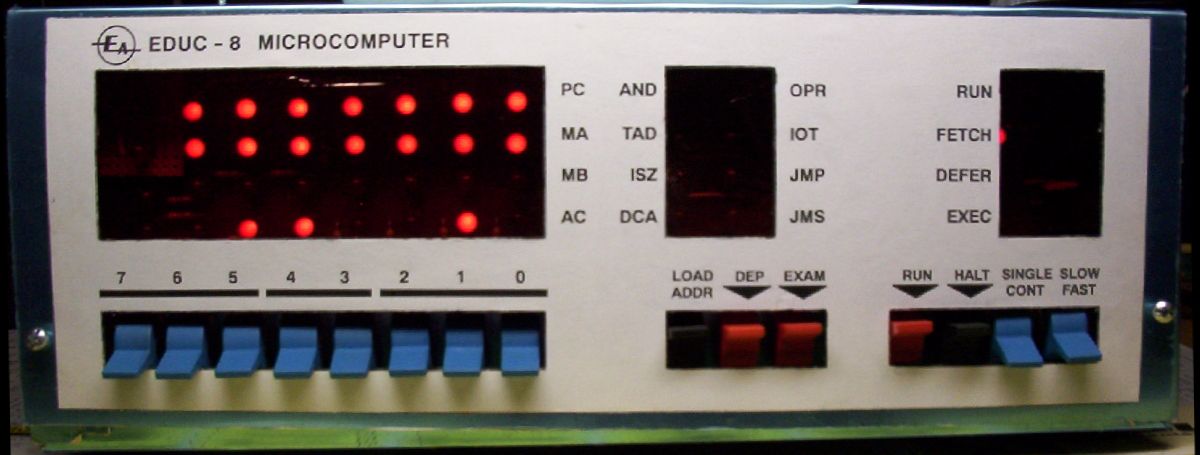
With another 7400 soldered in, the computer passed all the following tests! The last test is a simple program to increment AC to 255 and then stop. The photo at the top of the page shows this test being run. This worked perfectly. However, the program stops with MA = 000 (in octal) instead of 010 as described in the text. The cycle and instruction timing table given in the September 1974 issue of Electronics Australia shows that MA is cleared during the execute cycle of the HLT instruction, so I believe my computer is working correctly.
The "first test" program only tests the ISZ and JMP memory instructions. I wanted to test the other memory instructions as well. This program tests the DCA, AND and TAD instructions. AC is set to all ones and is ANDed with IDX which is initially loaded with 1. IDX is then left shifted once and ANDed with all ones again. As the program halts after every AND, pressing the run key should see a one shift lefted in AC one position.
00       CLA.IAC   711
01       DCA IDX   312
02 HERE  CLA.CMA   714
03       AND IDX   012
04       HLT       721
05       CLA       710
06       TAD IDX   112
07       RAL       702
10       DCA IDX   312
11       JMP HERE  502
12 IDX             000
The computer ran this progam OK. I then wrote a program to test the TAD better (instead of adding to just zero in the above program), as well as testing JMS and indirect addressing. In this case, AC should increment by one on the first press of run, and by two every time after.
00       CLA.IAC   711
01       DCA IDX   305
02 HERE  TAD IDX   105
03       HLT       721
04       JMP TMP   506
05 IDX             000
06 TMP   JMS SUB   410
07       JMP HERE  502
10 SUB             000
11       TAD IDX   105
12       JMP I SUB 530
Again, the program worked perfectly. I also tested the first run program starting at F0 in hex. This checked the upper memory chip. So everything appears to be working normally! I'm well pleased. The next task is the interface board. This will complete the EDUC-8 microcomputer.
24 August 2007. My EDUC-8 microcomputer is finally complete! Today I fininshed the E8/IOT board, as described in the January 1975 issue of EA. Not much to say, as we can't properly test the board until we have something to interface to. This will be the simple keypad and octal display, also described in the January 1975 issue.
 |
E8/IOT |
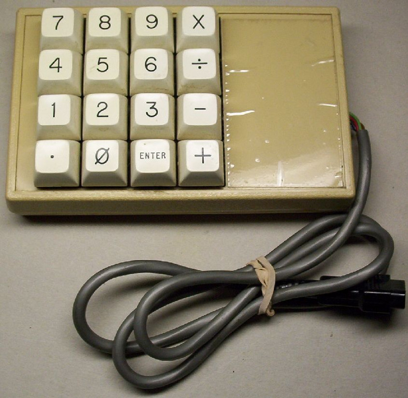
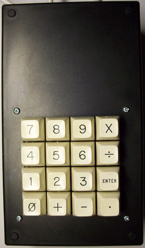
7 September 2007. This is an update on the EDUC-8 keypad. This is unfortunately not working yet. I was not able to find the original Mechanical Enterprises SK760 keypad. So I bought a keypad designed for the Commodore 64 from eBay.
 |
Commodore 64 keypad |
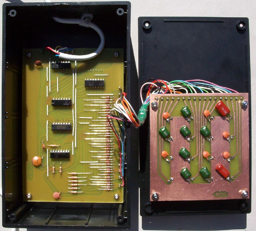
Opening the box, I found the keypad soldered to a PCB which also had a diode network soldered into it. I needed to attach the keyboard to the case lid, but the original PCB did not have any room for mounting holes. Thus, I decided to make a new PCB for the keypad. I first unsoldered the keypad using solder wick. I had to use a lot of wick, as there were 32 pins to unsolder! I then designed a new PCB, following the pin pattern of the SK760. This pattern is included in the PCB artwork in the Resources section. I made the board in only a few hours. I also fixed my laminator, which was not moving the rollers properly and making an annoying clicking noise. The screw holding the rolling motor had come loose.
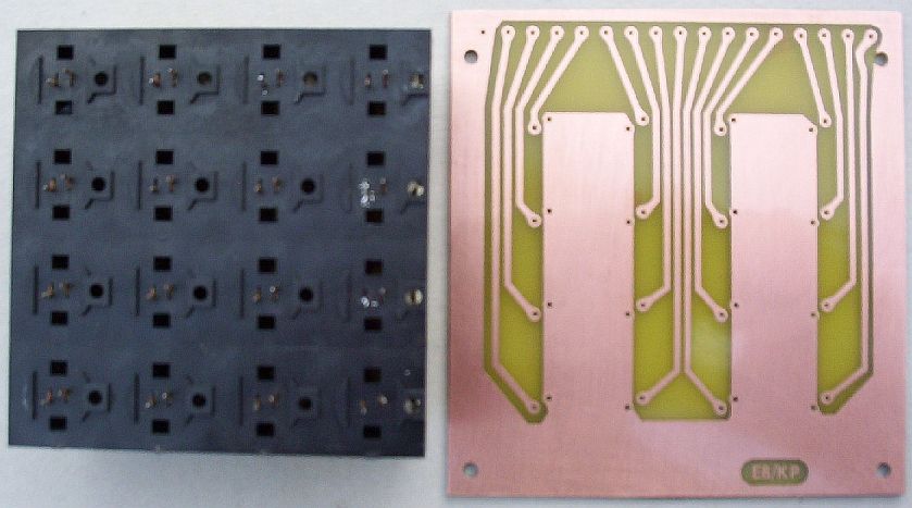 |
Unsoldered keypad next to PCB, labelled E8/KP. |
I initially made the keypad holes 1.0 mm in diameter, but when I tried to insert the keypad, one of the pins disappeared. I immediately thought I had broken the pin off. I widened the holes to 1.2 mm where another two pins disappeared. Finally, I widened the holes to 1.6 mm, before the keypad would fit. I soldered a wire to each of the broken pins. After soldering in the PCB pins, the keypad was inserted. I found that the keypad pins were not of an even height. The pins are very short, and just poke through the PCB. Removing a key, I examined the switch contacts and noticed they were not of an even height. Pushing on the pins must have pushed some of them slightly in. For the pins that had disappeared, this was only because the pin had been pushed in nearly all the way! Using a pair of pliers I pulled the pins back in place.
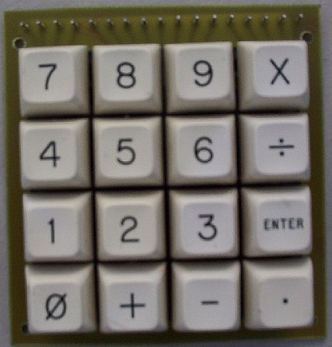 |
Completed keypad. Note that some keys have been switched to match the SK760. |
The PCB for the electronics was put together relatively easy. I just had to make sure I soldered in the diodes the right way. I used a plastic box from Dick Smith for the case and six-wire alarm cable for the cord. Once completed I plugged the keypad into IDO (input device zero) and checked that ground and +5V were wired correctly to the keypad.
 |
Completed keypad electronics. |
I wrote a simple program to transfer the contents of the keypad to the accumulator.
00       CLA       710  Clear Accumulator
01       RKF0      604  Clear IDO Flag
02 HERE  SKF0      601  Skip on IDO Flag
03       JMP HERE  502
04       KRB0      606  Read IDO and clear flag
05       JMP HERE  502
Not surprisingly this did not work! I got out the extender board so that I could check the IO board. I found that the FLAG FF on the keypad was always low (data ready) and was not being set by the RKF0 instruction. In slow mode, the clear signal (active low) was going to the rear connector, but not to the keypad. Aha! I had wired the connector for the keypad backwards! The connector has a symmetrical pattern with +5V and GND in the middle, so those pins do not get swapped.
 |
Inside the keypad box |
Fixing this problem, the keypad still did not work. The FLAG was still always low. The input to the FLAG buffer was only 1.66 V, an invalid level. I traced the fault to pin 6 of the 7400, where the output wire inside the chip seems to have broken. That's the fifth faulty 7400 chip I found! This time, this was a TI chip made in El Salvadore. The date code is 249B. This could be the 24th week of 1989, as the chip looks new, without the corrosion I normally see on chips from El Salvadore.
After replacing the 7400, the FLAG FF was now working correctly. However, in pressing the zero key I would get semi random results, instead of all zero. I would get decimal seven, three, one or zero. I suspected that this would be due to the keys bouncing. The original keypad used mercury bounceless switches. I only found this out when I read the article before building the keypad.
After the keypad register is cleared from a clear flag instruction, the 5-bit register would always go to 15 (01111 in binary) after pressing the zero key, instead of staying at zero. Examining the asynchronous parallel load (PL) input to the register, I could see this signal going momentarily high when the key is pushed down and also when it is released. The problem is when the key is released, since this will cause 15 to be loaded.
To fix the problem, I would need to design a debouncing circuit. I found this excellent tutorial on debouncing circuits. All that you need to do is add a capacitor across the switch and have the switch input connected to a Schmitt trigger. The diode matrix encodes the 16 switches into five bits. However, only four of those bits are used to trigger the one-shot that drives the PL signal. I though of placing capacitors at these four inputs, but decided that wasn't a good idea. Pressing a key would cause the capacitor to discharge directly into the diodes, with no resistor to absorbe the energy. Thus, 15 of the 16 keys would need a capacitor across the switch. The CTRL key (bottom right hand corner) is not used by the triggering logic.
I designed the time constant for the circuit to be 1 ms (the RC value), as recommended by the tutorial. Each of the four pullups is 27 kΩ. However, each key can be connected to either one, two, three or four pullups in parallel through the diodes. Thus, one pullup requires a 37 nF capacitor, two 74 nF, three 111 nF and four 148 nF. The closest standard components are 33, 68, 100 and 150 nF, respectively. We require 1, 7, 6, and 1 of each value, respectively.
The next problem was more difficult. How to insert Schmitt triggers into the four inputs? The standard 7414 Schmitt trigger has six inverters. I would need to insert a 7414 and then a 7400 or 7404 to get non-inverted data. Another solution was to replace the 7400 with a 7414 and completely rewire the PCB. The register would directly store the inverted data from the 7414. The DATA output would use only one (instead of two) of the 7437 NAND gate drivers, with the FLAG RESET input going to a spare 7414 inverter, instead of a 7437 gate. This frees up two 7437 NAND gates for the FLAG FF.
The two NOR gates for the MSB would disappear, and the two NAND gates for the trigger circuit would be replaced with NOR gates. One gate would go the inverted input of the one-shot, with the other going through a spare inverter into the non-inverted input. I spent a day drawing up a PCB board to do this! In researching Schmitt trigger IC's, others that are available are the 7413 dual 4-input NAND gate and 74132 quad 2-input NAND gate. Having now become very familiar with the circuit design, I realised that if we replace the 7400 with a 74132 (which are pin compatible), then this would directly provide the Schmitt trigger inputs! (This is a good example of how my mind works. I very slowly work out a very complicated solution, before realising the obvious simple one!)
I've ordered the 74132, four replacement 7400s and capacitors from Futurlec. The component costs are more expensive than Unicorn Electronics, but they have much cheaper postage since they are based here in Australia ($4 compared to $20). I'm still waiting for the parts to arrive. My next report will hopefully be a short one if all goes well with the design fix.
13 September 2007. The keypad is working! Yesterday, I received the components I ordered from Futurlec. Surprisingly, the parts were shipped from Thailand, although the invoice slip had Broadmeadow, NSW, Australia as the address. I desoldered the 7400 and replaced it with the 74132. The capacitors were soldered across the switch contacts, to minimise stray currents when they were shorted out by the switch.
 |
Modified keypad |
Running the test program, the keypad did not work properly. When pressing zero, instead of loading zero, seven would sometimes appear in the AC register. I checked the 7496, and could verify that it was being loaded with 15, instead of zero. Checking the PL input, I could not detect any pulses when the switch was lifted. I added a 100nF in parallel across the switch, and this seemed to do the trick. Zero was loading correctly. The other keys were also working most of the time, but that AC was being shifted to the right once. I later realised that I had swapped the 150nF capacitor for key zero with the 33nF capacitor for key seven. I fixed this, so that key zero only required a 150nF capacitor. However, key seven needed a 100nF capacitor in parallel, to make it work properly.
Checking the circuit diagrams, due to the inverter for CLOCK, data was being shifted out the 7496 register on the falling edge of CLOCK. However, the AC register inputs data on the rising edge of CLOCK. Since CLOCK is initially high, this means that the keypad register is shifted right (losing the LSB data), with the next bit being clocked into AC! This explained the shift right errors I was seeing. The fix was simple. I cut the track from the CLOCK input pin to the 7437 gate and from the gate to the wire link it goes to. I then soldered a link between the input pin and the wire link under the board. This meant that the keypad register was right shifted on the rising edge of CLOCK. Due to gate delays from the keypad register to AC, the data would last long enough to be clocked into AC. I have modified the PCB artwork with this correction.
Testing this modification, the keypad worked as expected, although some bits for some of the keys would not load correctly as before. If this happened while testing a key (pressing it down fast repeatedly) I would add an extra 100nF capacitor across the switch pins. At most only one extra 100nF was required. Thus, I would recommend using 150nF for each of the switches. In testing, if that is not enough, add an extra 47nF or 100nF. With these modifications, I managed to get the keypad working perfectly. I also tested both ID0 and ID1, to verify that both input ports were working.
 |
Completed keypad |
I'm a bit puzzled as to how the error with the CLOCK inverter occurred. James Rowe had built up the keypad, but does not give any test instructions. Did Jim actually test his design? If he had tested it, he would have found the error, just like I did.
9 November 2007. A long time since my last update, but I have got my EDUC-8 Octal Display working and have written some test software. I received a reply from Jim Rowe about the design error in the keypad. He says he doesn't remember why the correction was not shown in the magazine article, but the change was crudely made to the EDUC-8 booklet that was published.
 |
E8S board loaded |
The Octal Display went together pretty easily. The only difficulty was in finding suitably longs screws to mount the board. I ended up ordering M4 50 mm screws, nuts and washers from RS Components. The only screws I found in hardware shops were nearly all imperial. There were 3/16" (4.76 mm) 50 mm screws, but I preferred to use the smaller diameter M4 screws from RS. I could not find any M3 or 1/8" (3.18 mm) 50 mm screws.
 |
Octal display wired |
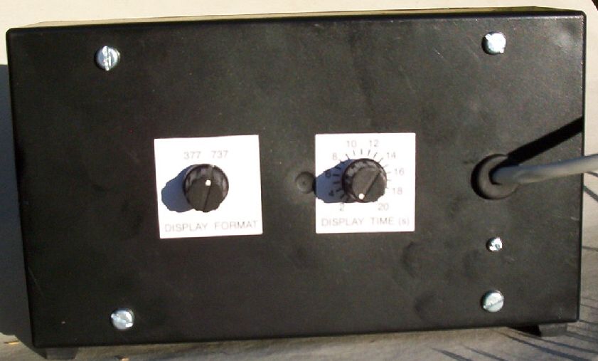
I also made up labels for the front of the unit and the two controls at the back. One control is used to select between 737 and 377 display. The other control can be used to change the display timing. These labels are included in the resources section below.
 |
The board mounted in the box. |
I connected the display to the computer and wrote a little program to test it. However, this did not work as I did not realise that writing to an output device also clears the accumulator. My second program corrected this and counts from 0 to 255 and then stops, using the timer in the display to control the time between each increment of the counter. Both output ports and the octal display worked perfectly. I also found the octal display to get quite warm! The old LED displays use quite a bit of power. My test program is below.
 |
Octal display controls. |
I then read the Electronics Australia article from February 1975 describing various programming techniques. I tried all the test programs. One test program that adds eight numbers stored in eight address locations used a technique that I had heard of, but not actually seen implemented. This is self-modifying code! The TAD instruction used to add the numbers is modified so that its address changes to the next number. However, the program as written will not work due to the 16 word page limitation. Ignoring the first CLA instruction which does not require memory addressing, the total number of instructions and data is 17, one greater than the page. I fixed this by moving the CONST value to the start of the program and starting the program at address 15 (I will refer to all address in 737 octal notation). The program needs to run from start address 16. The modified program is below.
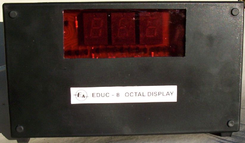 |
Front of the octal display. |
The next program that does a similar job, but with a pointer, can not be started from any location. Not including the first CLA instruction and the eight data locations, the program just fits into one page of 16 words. Thus the program should be started from address 17. Since a pointer is used the eight data words can be in the third page (or the first page if desired). This program is also given below.
The next program I wrote was used to test all the memory locations. This was a good experience into how the 16 word page size can be overcome. A good solution is to store all the constants, variables and addresses (data words) at the end of the page leaving the last word free. You start writing instructions from the start of the page with data words being stored from the top (leaving the top word free). When there is only one word left near the middle, you jump to the end of the page (address 17), where you can execute another instruction, or have a NOP if necessary. This then takes you into the next page, where the process repeats.
If the last middle instruction is conditional (ISZ, SZA, SMA, SKF, or SDF) then this technique won't work as the skip will be into a data word. The solution is to replace the conditional instruction with a jump to address 16. The data word at 16 is moved to just after the jump instruction. This leaves two words free at the end of the page for the conditional instruction and the following instruction.
The memory program also showed the limits of pointer addresses. Since you are doing an indirect on the pointer address, all instructions that change or use data at the address of the pointer must be in the same page as the pointer. If your instructions are spread over two pages, there are two possible solutions. One is to copy the pointer address into the next page. Another is to use subroutines to change or use the data. For the memory tester, I chose the later. The pointer address is stored in the last page. A subroutine used to write and read data to the pointer is also in this page. A general solution is to have a subroutine for each address instruction to the pointer address. Since each subroutine requires three words (return address, instruction, return instruction), we could have five subroutines for five instructions, e.g., AND, TAD, ISZ, DCA, and JMP plus the pointer itself.
In my memory test program I use the above techniques. I first clear and read the memory location to be tested, and test that is has been cleared correctly. I then test with all ones and then with all zeros. If the program ends at address 025 then the test is successful. If the program stops early, then the stopping address, the contents of the pointer address SAP, and the contents of the accumulator will help work out which address location is at fault. In my test, all addresses tested perfectly. The program is below.
The nest program I'm going to write is to use the keypad and octal display to enter and examine programs.
2 December 2007. I've written a program that can be used to write and read programs using the keypad and octal display. After several iterations, my first attempt used nine pages (144 words), taking up more than half the available memory! Using some tricks, I was able to squeeze this into seven pages (111 words) without any loss of functionality. This leaves nine pages free to write your program. Although limited, I found the instruction set to be very powerful and compact. I don't think any modern CPU could achieve the same functionality with less than 110 words.
The software is given in the resources section. Instructions for using the code are given with the program. In my first attempt, I misentered an instruction, which resulted in some wild program execution. After correcting this, the program worked perfectly! I was able to enter, examine, and run a program I entered through the keypad. I was even able to examine the Octal Display Program itself, after loading its starting address of 420.
I learnt a lot from writing this program. Due to the 16 word page, making a change results in a lot of work in shifting the instructions, constants, addresses and variables. In future, I am first going to write some pseudo code, similar to a high level language. I would then translate this into EDUC-8 instructions, but ignoring the 16 word page limit. For variables that are used as pointers, I would either try to have the indirect instructions close to the variable (to stay within the 16 word page), or use subroutines. I would then translate this into proper assembly language, where the 16 word page limit is considered. This means a lot of indirects for reference to the variables.
One trick I used is when there is a test instruction, like SZA (skip on zero accumulator). The skip would go into the next program section and then would jump back to the start of the program, to input the next character. The instruction after SZA would be a jump into the next test. Instead of jumping to the end of the program section, we jump to the end of the constants, addresses, and variables (CAV) section. The CAV section starts at the end the program section. This results in the CAV section being in the middle of a page. At the end of each program section and its CAV, we count the remaining words in the page. We then count the following instructions, adding words to the CAV as required, until the end of the page is reached. I found that each page usually has five to seven words in each CAV section.
I went to HC Robinson's last week. This is a very old electronics store that has been in business for over 60 years! The owner (Robbie) is getting very old though and only opens the store on Tuesday and Saturday mornings. There is a huge amount of old electronics in the store, and is like venturing into an Aladdins cave. You will never know what you will find. I was able to buy an old keyboard that has a single pole single throw (SPST) switch for each key. In fact, the keys are of the exact same type as my keypad. I was also looking for a paper tape punch and reader, but Robbie could not find one. If anyone knows where I can get a paper tape punch and reader, that would be much appreciated.
The next program I would like to write is a simple calculator.
25 January 2008. I've finished writing a calculator program! This started off as an eight digit calculator with decimal point, addition, subtraction, multiplication and division. Due to memory limits, the first to go was the decimal point. I wrote the program in Pascal and then started to hand convert this to assembly. This time, I ignored the page constraints, which make programming much easier.
I soon realised that multiplication and division would have to go as well. The next step was to break the program into 16 word pages. This was followed by the addition of the constants and variables into the pages, the labeling of each line with its address in 737 format, and then finally the conversion of the code into 737.
My first attempt used 255 bytes. Programming took me about 20 minutes! As I was using the octal display, only one digit could be displayed at a time. Pressing a number on the keypad would store this into the display register, increment the pointer, which would display the next character. I didn't like this and decided to have another go. I also simplified the program by replacing the subroutines used for indirect TAD and DCA by careful placement of these instructions within a page. This saved about a page, which I used to add the ability to show under and overflows.
This second attempt resulted in a size of 253 bytes. The display pointer would now decrement, but only when the ENTER key was pressed. CTRL(ENTER) was used to perform the calculation. Entering a number, the pointer would stay the same. I didn't like this either, as ENTER had to be pressed after each number was pressed. Also, I found a bug. Minus zero resulted in the inversion of the result. This could be fixed, but required six words, and I only had three spare!
By reducing the complexity of how the overflow is calculated, I found sufficient memory. Also, I changed the input to be similar to the first scheme, except now the pointer would decrement, so numbers could be entered most significant figure first. The program now worked to my satisfaction. The code is below.
I found having to re-create the assembly after each change to be quite tedious, especially when you are using nearly the entire memory of the computer. Therefore, my next task is to write an assembler program.
11 February 2008. I've finished writing an assembler program. The program is written in Pascal and compiled used Free Pascal for 32-bit DOS. The program is a lot more complicated than what I thought it would be, being 670 lines in total. You still have to organise the program words to fit into each 16 word page. I left this to be done manually as instructions with indirect variables need to be on the same page, and shuffling instructions around can avoid blank lines being inserted, making most use of the words available. I've tested the program with sources for my octal display and calculator program. The compiled code was input by hand into my EDUC-8 and worked perfectly. You can download the software (including the pascal source) from the Programs section below. The next program I'm going to write is an 8 digit multiplier, followed by an 8 digit divider.
23 December 2008. I've finished writing the multiplier program, available below. After finding one bug, the program worked perfectly. I had to enter the program three times to get it to work, which is a bit tedious to say the least. Next up is the divider program.
2 January 2009. It took awhile to get the bugs out, but I've now written a program that does eight digit division and modulus operations. The multiplier and this program were written in assembly, and then assembled using e8asy. Using e8asy certainly makes writing assembly code easier, compared to the manual process beforehand. I found one bug, which required two bytes to fix. Fortunately, there were two unused bytes in the page where the error was, so only that page had to be corrected. The program takes 253 bytes (only three bytes spare) and I made four errors in programming the EDUC-8. I found two errors during my first check. The other errors were found when the program didn't work correctly, and I went about checking the code again. My next program is going to be either a four or eight state Viterbi decoder, depending on how much space the program takes.
24 February 2009. Tomorrow I will be presenting a slide show, available below, of how I built and programmed the EDUC-8 computer. This will be presented at the Institite for Telecommunications, University of South Australia, Mawson Lakes, where I have an adjunct position.
1 May 2009. I've done it! I've written a Viterbi decoder program using every byte of the EDUC-8 memory. A Viterbi decoder uses a complicated algorithm for decoding information transmitted using a convolutional code over a digital communications channel. The decoder is able to correct many errors caused by noise, interference and distortion in the channel. There was just enough room to decode a simple rate 1/2 four state code using soft decisions. Four bit signed magnitude received quantisation is used, with a maximum magnitude of nine. The traceback depth is 16 and the decoder delay is 18. I spent a day and a half testing and debugging the decoder. This morning I made the last correction and verified that it is working with a test received sequence.
To write the program, I made some updates to the EDUC-8 assembler. This includes the initialisation of variables as well as allowing direct references to an array or table within a page. I've also updated the simple write program to write2, so that it can now perform read and write operations, displaying the index address in AC.
The next program I want to write is calendar day calculator.
7 May 2009. I have successfully written and tested my Calendar program. This uses 15 pages and works very well, not making any mistakes for any of the dates I tried. As always, I found a couple of bugs in the program while testing, but these were easily fixed. The program is included with e8asy. This is a fun program to run. It would have been good if the EDUC-8 octal display had a decimal display option so that the day, month, century and year could be displayed two digits at a time, instead of one digit (in octal) at a time. The 377 option on the display is fairly useless, as I always use the 737 format for programming the computer and displaying data.
Now having written several programs the next step is to interface to my Facit 4042 paper tape punch and reader. My machine has a serial interface, so I'll be using the EDUC-8 SR-T board which has a UART. So the next step is to build up that board, along with another PCB for the -12 V power supply for the UART, teletype interface and magnetic tape interface.
 |
29 February 2012. David Snelling in the UK successfully built an EDUC-8 using the PCB plans from this web site and some parts we supplied (switches and connectors). The box to the left is the power supply. |
 |
9 January 2013. John Clarke from New Zealand started his EDUC-8 in 1975 by obtaining original EDUC-8 PCBs, connectors, front panel, case, some ICs and handbook. However, university, a lack of funds and not knowing where to buy all the parts meant the project was put away. Recently digging out his EDUC-8 parts from his garage and finding this website has allowed John to finish his EDUC-8. In test rig. Inside case. |
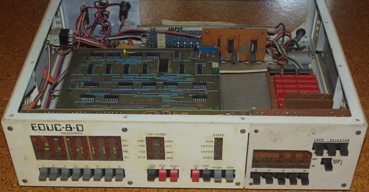 |
12 April 2013. Harry Sokol from Australia built an EDUC-8 in the 1970s with the Jim Rowe IO expansion. The upper 1024 bit RAM was replaced with several banks of memory, each bank with 128 bytes of RAM. The additional switches on the right are used to load the address of the memory bank, output and input ports before booting the system, allowing selection of which memory bank is initially active. |
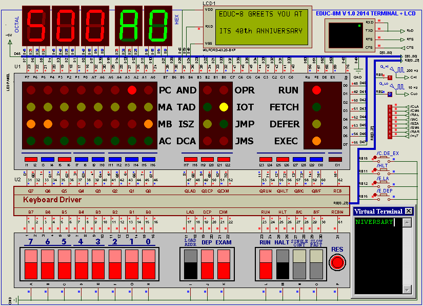 |
19 June 2014. Lavr Semionovich from the US has designed a software model of the EDUC-8 using Proteus Project, Labcenter Electronics and Professional PCB software. The image here gives a message to celebrate EDUC-8's 40'th anniversary this year. |
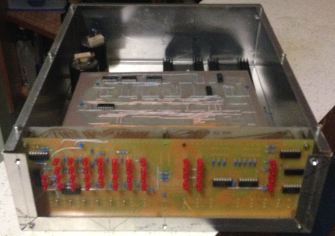 |
30 June 2014. Gwyllym Suter from Australia is building an EDUC-8 using the PCB layouts from this website. This is the current state of construction. Here are the boards on 1 April 2013. 1 July 2013: Back, Front, Front Panel, and Front Panel socket pins. |
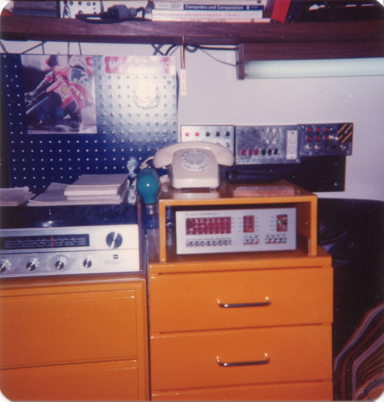 |
14 August 2014. Ray Hollingworth from Australia has shared this photo from the late 1970's of his bedroom where his EDUC-8 can be seen. |
 |
18 August 2014. Here is Hugh Buckle's EDUC-8 which he built in the 1970's. Hugh placed his EDUC-8 in a frame with an attached keyboard. |
 |
7 January 2019. Here is Anthony Nixon's EDUC-8 hardware emulator. This is a single board using a PIC and some memory to replace the original design. It can also emulate the Page Zero modification and a What If modication that increases the number of instructions from 28 to 56. You can build your own copy of the emulator from Anthony Nixon's web site |
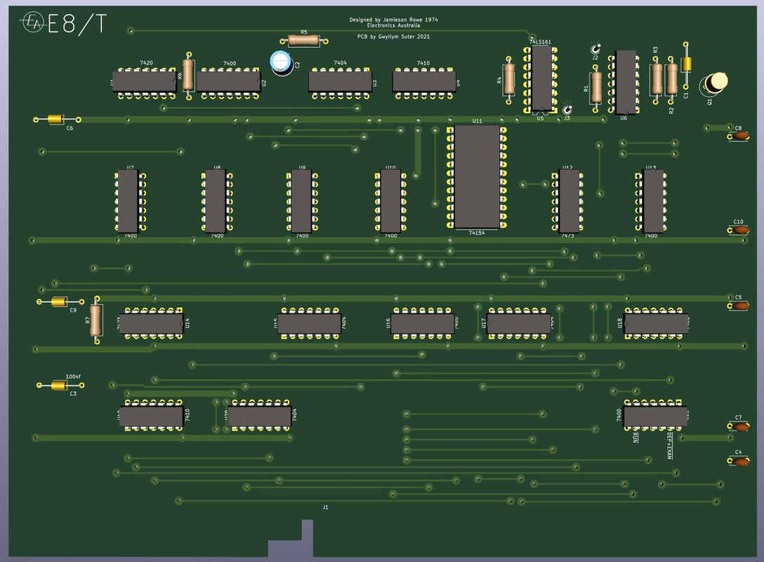 |
22 July 2019. Updated 30 June 2021. Gwyllym Suter has completed his EDUC-8 PCB design project and has updated his design to use edge connectors, instead of D-type connectors. At left is a computer drawn image of the timing board. He's also completed a PCB for the power supply. The memory board has the Page Zero option added. Schematics and gerber files for all the boards can be found in the resources section. You can download a computer animations of the completed boards and Octal Display. Gwyllym is currently having 10 sets of boards made and will have them on sale from Amazon. You can download the Kicad schematics and PCB artwork here. Here's the new front panel. |
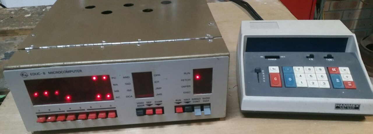 |
23 May 2020. This is Johannes Roggeveen's original EDUC-8 that he built in the 1970s. He used it originally for controlling a hydroponic vegetable garden and recently for controlling Christmas lights! The full image also shows the calculator that is used to contain the EDUC-8 keyboard electronics. |
 |
16 May 2021. This is Ian Jenson's parallel implementation of the EDUC-8 that he built in the 1970s. The computer only used 60 IC's, compared to 100 with the original serial design, had expandable memory up to 4 KB and an interrupt system! Views inside the "CPU" are here and here. Ian has also kindly agreed to make public his original schematics which you can download here (updated 14 Aug. 2025). |
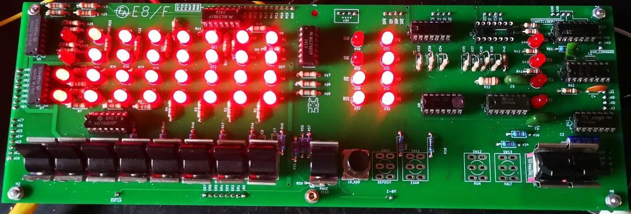 |
25 January 2022. This is Gwyllym Suter's Front Panel that he is building for the ACMS. More construction photos can be found here. |
 |
1 March 2023. Dale Hughes from Canberra is currently building a machine using 74LS and 74HC logic on Vero boards. A photo of the inside of his machine is here. |
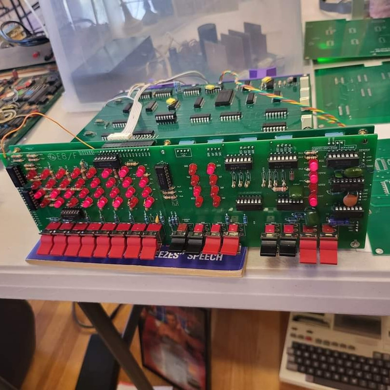 |
25 April 2023. Gwyllym Suter displayed his EDUC-8 at the Canberra Vintage Computer Exhibition 2023 on Saturday 22 April. Other images are here and here. |
 |
14 Jan. 2024. Gwyllym Suter's new PCB's in custom 3D printed case. Other images are here and here. |
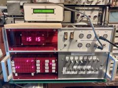 |
20 Feb. 2024. Dale Hughes has his expansion working with 64KB of RAM and 3 I/O ports. Dale used Rowe's original I/O expansion scheme which allows 16 input and 16 output ports. However, only three external I/O ports are implemented. Two outputs are used to write the low and high address of the 16-bit address. RAM is implemented using two 32Kx8 SRAMs. One output port is used to write 8 bits of data and one input port is used to read 8 bits of data. 48 bytes of main memory (256 bytes) are used to read and write programs to and from main memory. |
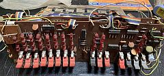 |
4 May 2024. This is Ken Rayner's original machine that he built and got working in 1978. It is currently being restored by Gwyllym Suter. Here are pictures of Ken's Front Panel, E8/T, E8/T PCB, E8/D, E8/A, E8/A PCB, E8/IOT, E8/IOT PCB and EDUC-8 book |
 |
31 May 2024. Dale Hughes is currently building a machine using the boards from Gwyllym Suter. Here is the E8/C Motherboard. 7 June 2024 update. Dale has his machine running! Here's a video, the front, bottom and top during testing. |
EDUC-8 Electronics Australia articles by Jamieson Rowe
Part List
Order List
Power Supply Circuit Diagram, Flying Lead Labels, Keypad and Octal Display Labels
Front Panel Artwork
Printed Circuit Patterns
Slide Show: "Building and Programming Australia’s First Hobby Computer, the EDUC–8", by Steven S. Pietrobon, 25 February 2009.
Page Zero Implementation for EDUC-8, by
Steven S. Pietrobon, 23 March 2013. Updated 2 March 2023.
IEC format schematics by Lavr Semionovich, 20 June 2014.
OCR scans of EDUC-8 articles by Lavr Semionovich, 20 June 1014.
EDUC-8ME Memory and Input/Output Port Extension for the EDUC-8 Microcomputer, by Steven S. Pietrobon, 13 March 2023. Updated 15 May 2025.
Using Low Power Schottky (74LS) Logic for the EDUC-8 Microcomputer, by Steven S. Pietrobon, 29 March 2023.
EDUC-8L Adding a Link Bit to the EDUC–8 Microcomputer, by Steven S. Pietrobon, 7 June 2024. Updated 15 May 2025.
EDUC-8 Design Files by Gwyllym Suter, 19 Jul. 2025. Includes schematics in KiCAD and gerber files to make your own double sided printed circuit boards for EDUC-8 and EDUC-8 peripherals and EDUC-8 case in Freecad.
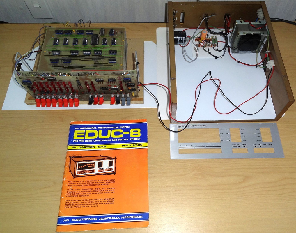
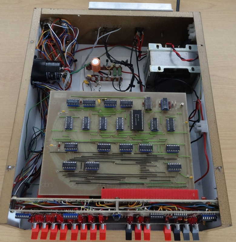
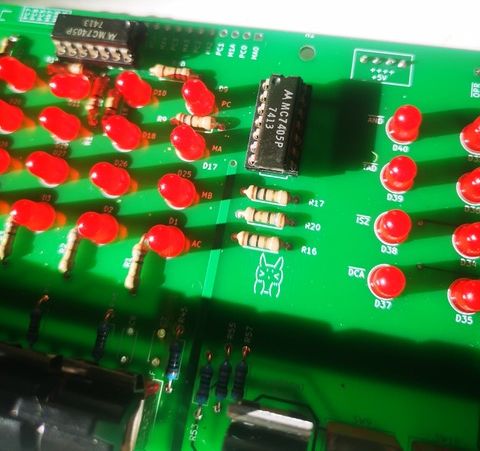
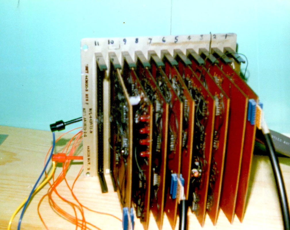
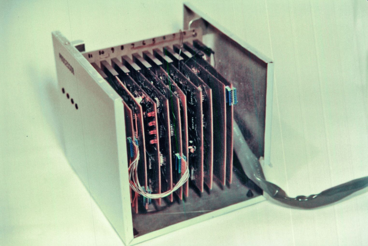
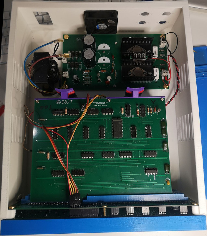
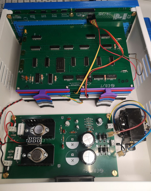
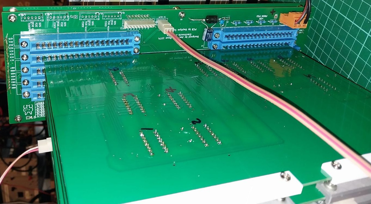
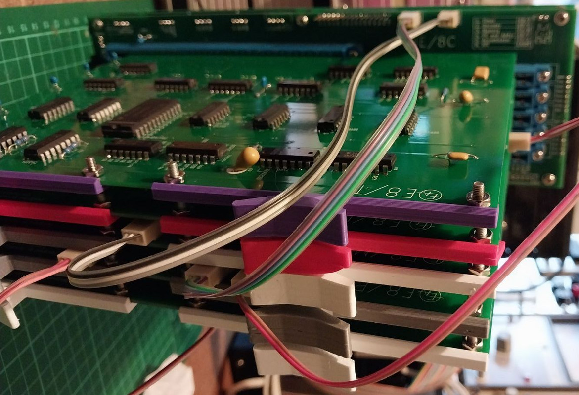